
This 17μA reset chip could be the 'stabilizing anchor' for your circuit board—the CD803.
Embedded microprocessors and MCU systems have become the core components in industrial control systems, smart instruments, and portable electronic devices. The operational stability of these systems heavily relies on stable power supply voltage monitoring and reliable reset mechanisms. Power-on sequence irregularities, voltage drops during power loss, and transient power fluctuations can easily trigger reliability issues such as program runaway, data errors, and abnormal module startup/stop operations. Current industry reset devices face common challenges including reset failure in low-voltage ranges, insufficient threshold precision, high static power consumption, poor multi-level domain compatibility, redundant peripheral circuits, and limitations in miniaturization design. These factors have become critical constraints on mass production stability and power management in embedded systems.
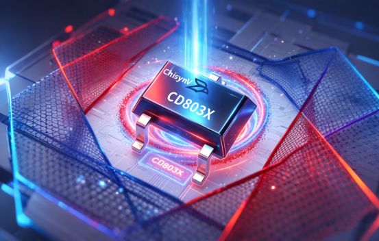
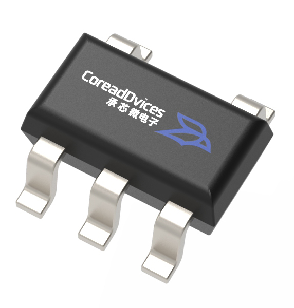
The ChisynV CD803X series is a leakage-output, low-efficiency reset power monitoring chip specifically designed for embedded systems. It focuses on low power consumption, high reliability, and broad compatibility in reset requirements, with robust electrical performance to ensure stable system operation. This chip serves as a standardized reset solution for engineers' hardware selection and mass production.
The CD803X features an open-drain output architecture with low-level effective reset signal (RESET), offering an output voltage range of-0.3V to +6V to ensure high compatibility with system reset topologies.
1. Reliability of High Voltage Power Supply and Low Voltage Reset
The device operates within a voltage range of 1.0V to 5.5V, maintaining effective reset output even when the supply voltage drops to 1V. This effectively resolves the failure issues of traditional reset devices under low-voltage critical conditions, preventing system instability during undervoltage or power loss scenarios. Additionally, it features a voltage tolerance margin of-0.3V to 6V, enabling robust resistance to power transient surges and compatibility with complex power supply environments.
2. ultra-low static power consumption
The device demonstrates excellent static power consumption control. When the supply voltage is below 3.6V, the typical static current is only 17μA, with a maximum of 30μA. At supply voltages below 5.5V, the maximum static current reaches 35μA. The extremely low power loss does not increase the battery life pressure for battery-powered devices, making it perfectly suitable for power-sensitive applications such as calculators, portable smart instruments, and low-power controllers.
3. Seven-level precise reset threshold
The CD803X features seven fixed high-precision reset thresholds, enabling accurate voltage monitoring without external calibration. It meets mainstream system power requirements: 4.63V and 4.38V for 5V systems, 4.00V for 3.3V/5V compatible systems, 3.08V and 2.93V for 3.3V systems, and 2.63V/2.32V for 2.5V/3.0V systems. These precise thresholds effectively prevent false resets and missed triggers caused by power fluctuations, ensuring stable system startup and operation.

4. Stable Reposition Timing and Output Characteristics
The power-on reset pulse has a minimum width of 140ms, typical 240ms, and maximum 460ms. The fixed timing ensures the power supply remains fully stable before releasing the reset signal, fundamentally preventing abnormal MCU startup upon power-on. The output maintains stable low-level characteristics: under low-current drive, the low-level voltage remains ≤0.3V; even under high-current drive, reliable low-level voltage is maintained with no reset trigger failure risks. In reset-inactive state, leakage current stays ≤1μA without additional power loss.
5. State controllability across the entire voltage range
When the supply voltage drops below 0.8V, the device output state can be stabilized by an external 100kΩ pull-down resistor, effectively eliminating CMOS logic input drift and enabling controllable reset states across the entire 0V–5.5V voltage range, thereby enhancing system reliability under extreme operating conditions.
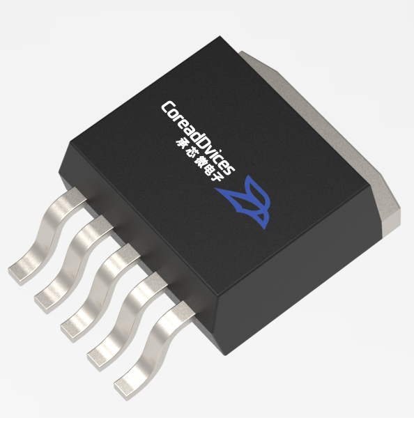
6. Packaging Specifications and Mass Production Compatibility
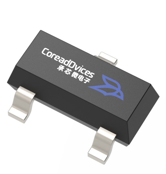
The CD803X series adopts SC70-3 ultra-compact packaging, designed to accommodate high-density PCB layouts and space constraints in miniaturized devices. The device operates within a temperature range of-40°C to 85°C, featuring stable parameter temperature characteristics and compatibility with industrial-grade application environments.
Application scenario implementation value
1. Portable low-power devices: Ultra-low power consumption characteristics effectively extend battery life, compact packaging accommodates space-efficient designs, and low-voltage reset functionality ensures stable reliability, comprehensively enhancing operational reliability of calculators and portable instruments.
2. Industrial Controller/MCU: Features stable reset timing and low-power consumption to ensure long-term reliable operation of equipment in industrial control scenarios, meeting the requirements of industrial-grade wide-temperature environments. System: Resistant to wide voltage fluctuations and power supply variations, with precise threshold settings to prevent false triggering. The open-drain output supports multi-module reset sharing, ensuring continuous operation of industrial equipment.
3. Hybrid level-domain system: Enables 3.3V/5V cross-domain reset without level conversion, simplifying circuit design and reducing BOM and debugging costs.
4. High-density miniaturized terminals: Ultra-compact packaging saves PCB space, with minimalist peripheries meeting the design requirements of miniaturized products.