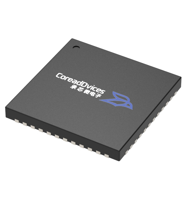
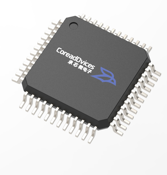
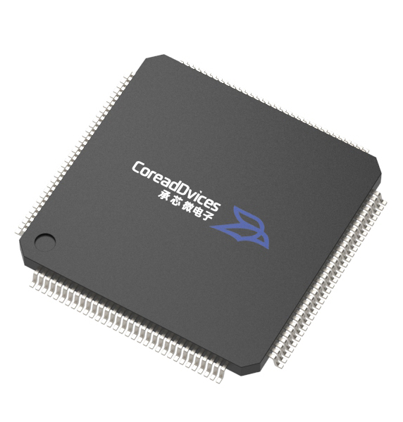
CD08AD1500 is made by CMOS process A semiconductor integrated circuit. This product combines folding and interpolation The circuit contains sample/hold amplifier
and folding Amplifier, bandgap voltage reference, clock circuit and LVDS output Etc. The circuit is packaged in a 128 lead four sided flat shell(TQFP128), overall dimension is 22mm × 22mm × 2mm, in accordance with GJB597A-1996.The product features high sampling rate, low power consumption, small linear error Automatic gain and offset correction and 3- wire interface control.Gain, offset and connection of internal circuit can be realized through 3-wire interface The clock matching between channels is used for correction, and the analog input is differential input,Either AC coupling or DC coupling; Clock input circuit internal With DC offset, AC coupling input is required. This product is compatible with foreign National Semiconductor companies The ADC08D1500 pins of the company's products are arranged in the same way, with the same function and performance It can directly replace ADC08D1500.

 CD08AD1500QPPrice:$0.00