CD96AD53-125
CD96AD53-125
RoHS
Quad, 16 bit, 125 MSPS serial LVDS 1.8V analog-to-digital converter
Active   |  Production cycle:
Products Selection
  • CD96AD53-125
    CD96AD53-125
    Price:$0.00

    Package:QFN-48

    Stock:0

    Package Qty:Tray, 260

    Price:
    1+   $0.00
    10+   $0.00
    100+   $0.00
    1000+   $0.00


Price:
Quantity:

Total:$0.00
Add to Cart
  • Resolution(Bits): 14
  • Channel:4
  • Interface Type: parallel LVDS
  • Sample rate(Msps): 125
  • Input Type: Differential
  • Structure Type: Pipeline
  • Analog Supply Voltage: 1.8 V
  • Digital Supply Voltage: 1.8 V
  • SNR: 74 dB
  • Operationing temperature range -40 ℃~+85 ℃


  • 1.8 V supply operation

  • Low power: 164 mW per channel at 125 MSPS

  • SNR = 76.5 dBFS at 70 MHz (2.0 V p-p input span)

  • SNR = 77.5 dBFS at 70 MHz (2.6 V p-p input span)

  • SFDR = 90 dBc (to Nyquist, 2.0 V p-p input span)

  • DNL = ±0.7 LSB; INL = ±3.5 LSB (2.0 V p-p input span)

  • Serial LVDS (ANSI-644, default) and low power, reduced range option (similar to IEEE 1596.3)

  • 650 MHz full power analog bandwidth

  • 2 V p-p input voltage range (supports up to 2.6 V p-p)

  • Serial port control

    Full chip and individual channel power-down modes 

    Flexible bit orientation

    Built-in and custom digital test pattern generation 

    Multichip sync and clock divider

    Programmable output clock and data alignment

    Standby mode


  • Medical ultrasound and MRI

  • High speed imaging

  • Quadrature radio receivers

  • Diversity radio receivers

  • Test equipment


Description
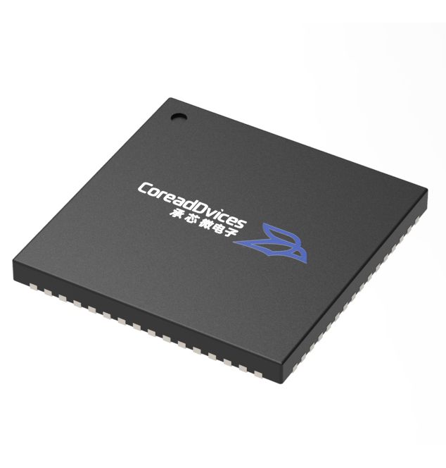
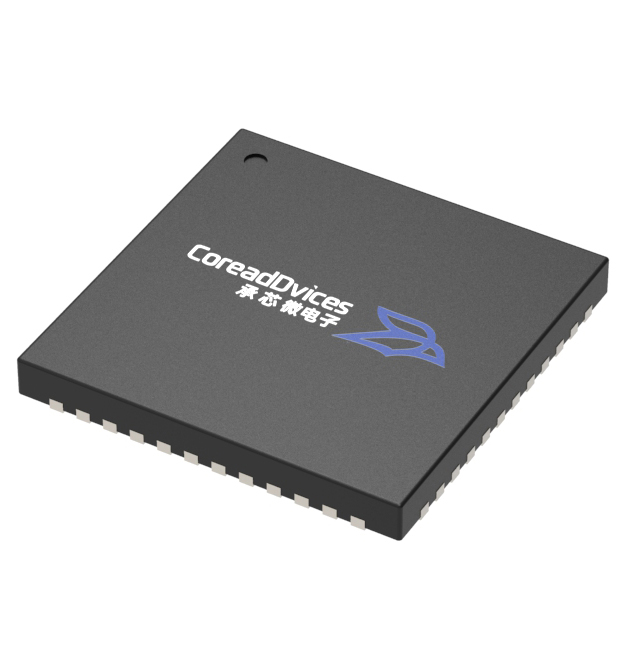
The CD96AD53 is a quad, 16-bit, 125 MSPS analog-to-digital converter (ADC) with an on-chip sample-and-hold circuit designed for low cost, low power, small size, and ease of use. The product operates at a conversion rate of up to 125 MSPS and is optimized for outstanding dynamic performance and low power in applications where a small package size is critical.The ADC requires a single 1.8 V power supply and LVPECL-/ CMOS-/LVDS-compatible sample rate clock for full performance operation. No external reference or driver components are required for many applications.The ADC automatically multiplies the sample rate clock for the appropriate LVDS serial data rate. A data clock output (DCO) for capturing data on the output and a frame clock output (FCO) for signaling a new output byte are provided. Individual channel power-down is supported and typically consumes less than 2 mW when all channels are disabled. The ADC contains several features designed to maximize flexibility and minimize system cost, suchas programmable output clock and data alignment and digital test pattern generation. The available digital test patterns include built-in deterministic and pseudorandom patterns, along with custom user-defined test patterns entered via the serial port interface (SPI).

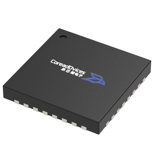
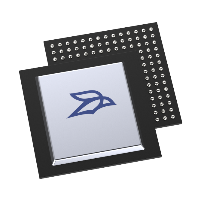
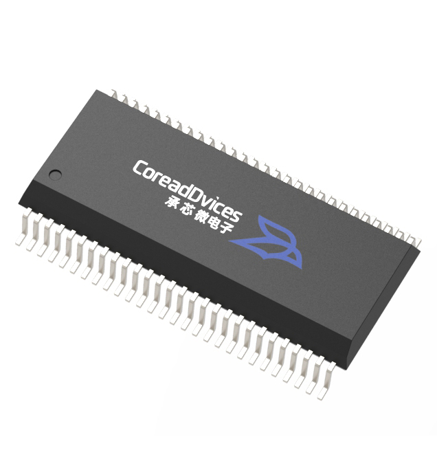
The CD96AD53 is available in a RoHS-compliant, 48-lead LFCSP. It is specified over the industrial temperature range of −40°C to +85°C.

Products Selection
  • CD96AD53-125
    CD96AD53-125
    Package:QFN-48 Price:

    Package:QFN-48

    Stock:0

    package Qty:Tray, 260

    Price:
    1+   $0.00
    10+   $0.00
    100+   $0.00
    1000+   $0.00

Price:
Quantity:

Total:$0.00
Add to Cart