Original part discontinued? Need alternatives?
Enter another manufacturer's part number, and we'll help you find equivalent, similar, or substitute ChisynV products.

-
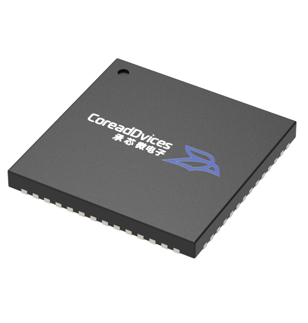 CD96AD56-125Price:$0.00
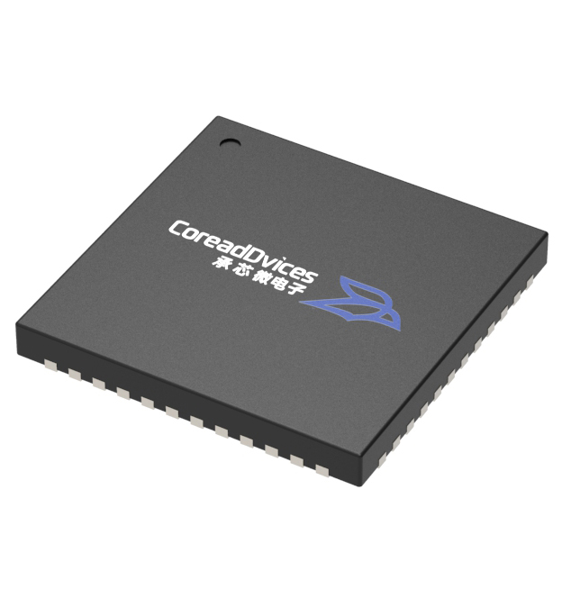
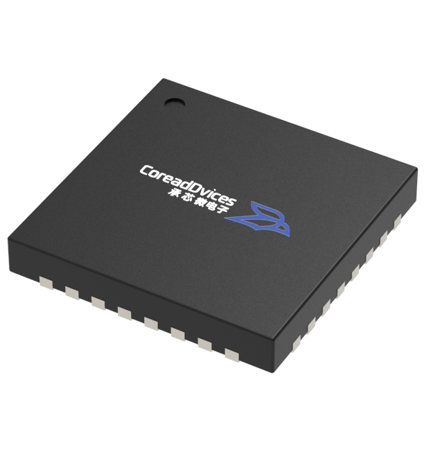
Package:QFN-56
Stock:1000
Package Qty:Tray, 260
Price:
1+ $0.00
10+ $0.00
100+ $0.00
1000+ $0.00
Price:
Quantity: