The CDRF9009 is a highly integrated, radio frequency (RF), agile transceiver offering dual transmitters and receivers, integrated synthesizers, and digital signal processing functions.
The receive path consists of two independent direct conversion receivers with 400MHz receiver bandwidth.
CDRF9009 also supports two observation path receivers (ORX) that can be used for digital predistortion (DPD) function.
The complete receive subsystem includes automatic and manual attenuation control, dc offset correction, quadrature error correction (QEC), and digital filtering, thus eliminating the need for these functions in the digital baseband.
The received signals are digitized with a set of interleaved pipeline ADCs that provide inherent antialiasing. The combination of the direct conversion architecture, which does not suffer from out of band image mixing, and the lack of aliasing, eases the requirements of the RF filters when compared to traditional intermediate frequency (IF) receivers.
The transmitters use a direct conversion modulator that achieves high modulation accuracy with exceptionally low noise.
The observation receiver path includes manual attenuation control, dc offset correction, quadrature error correction and digital filtering, thus supporting wide receiver bandwidth and high dynamic range.
The observation receive path supports 450MHz receive bandwidth, and can be used as wide bandwidth receiver without automatic gain control (AGC) function.
The fully integrated fractional–N frequency synthesis generates high performance local oscillator (LO) for receiver and transmitter, and clocks needed for the digital circuits, converters and serial interface.
Two integrated fractional-N frequency syntheses can be used for receiver or transmitter as RF local oscillator (LO), and frequency source for fast frequency hopping with ping-pong mode.
CDRF9009 supports multichip synchronization mechanism that synchronizes the phase of the RF local oscillator (LO) and digital clock.
The high speed JESD204B interface supports up to 12.28Gbps lane rates, and can be configured for receive data and transmitter data flexibly.
The power supplies of CDRF9009 include 1.0V, 1.2V, 1.8V and 3.3V.These voltages can be generated form linear regulators or switching regulators.
CDRF9009 uses an SPI interface to communicate with the external processor.
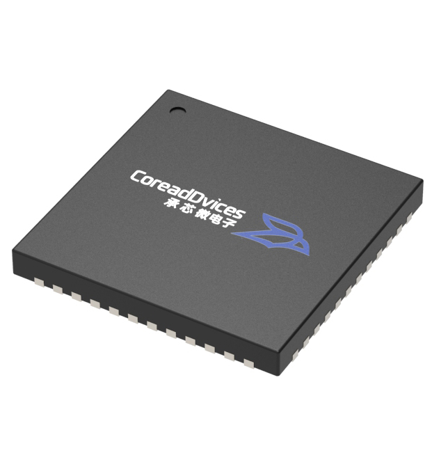
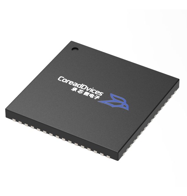
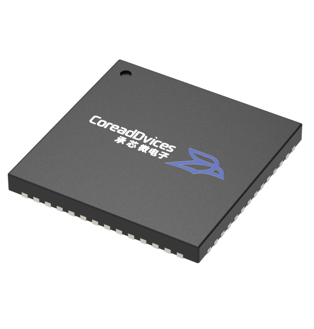
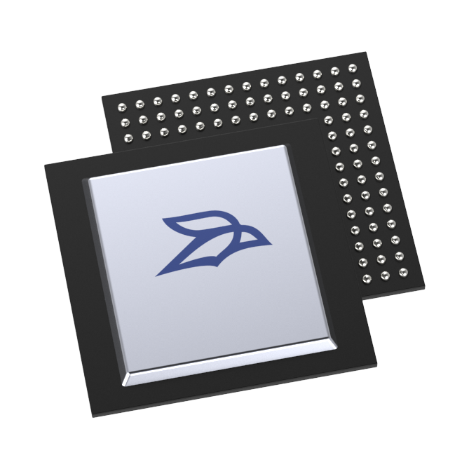
CDRF9009 is packaged in a 12mm x 12mm, 196-ball Flip chip ball grid array (CSP BGA).
CDRF9009 operates over extended industrial temperature range -40℃~+85℃.
CDRF9009 is compatible with and can replace Analog Devices, Inc.'s (ADI) ADRV9009BBCZ.

 CDRF9009BGPrice:$0.00