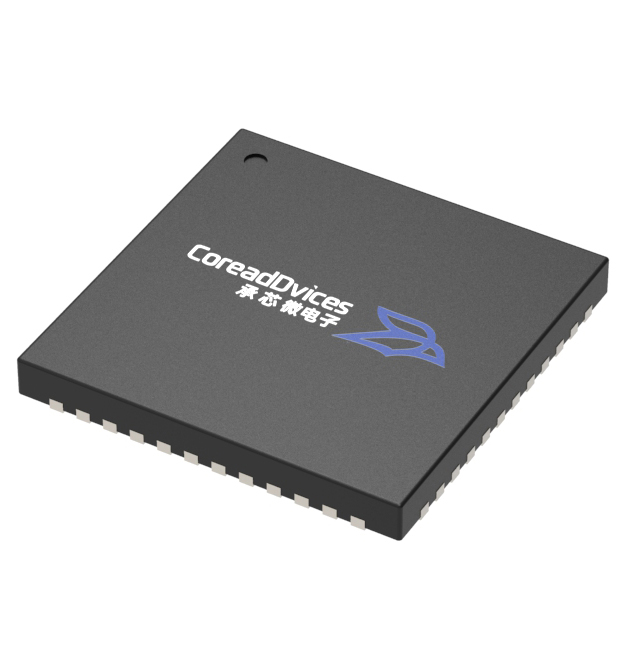
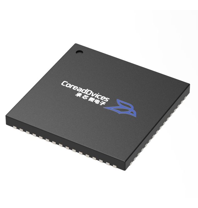
The CDRF9002 is a highly integrated RF transceiver offering dual transmitters and dual receivers, integrated synthesizers, and digital signal processing functions.
The CDRF9002 is a high performance, high linear, high dynamic range transceiver, and is extremely suitable for low power, portable and battery powered equipment.
The CDRF9002 operates from 10MHz to 7250MHz. The device is capable of both TDD and FDD operation.
The CDRF9002 consists of direct conversion signal paths with ideal noise figure and linearity. Each complete receiver and transmitter subsystem includes dc offset correction, quadrature error correction (QEC), and programmable digital filters, which eliminate the need for these functions in the digital baseband. In addition, several auxiliary functions, such as auxiliary analog-to-digital converters (ADCs), auxiliary digital-to-analog converters (DACs), and general-purpose inputs/outputs (GPIOs), are integrated to provide additional monitoring and control capability.
The fully integrated phase-locked loops (PLLs) provide high performance, low power, fractional-N frequency synthesis for the transmitter, receiver, and clock sections. Careful design and layout techniques provide the isolation required in high performance personal radio applications.
All voltage controlled oscillator (VCO) and loop filter components are integrated to minimize the external component count. The local oscillators (LOs) have flexible configuration options and include fast lock modes.
The transceiver includes low power sleep and monitor modes to save power and extend the battery life of portable devices while monitoring communications.
CDRF9002 supports multichip synchronization mechanism that synchronizes the phase of the RF local oscillator (LO) and digital clock.
The power supplies of CDRF9002 include 1.0V, 1.3V and 1.8V. These voltages can be generated form linear regulators or switching regulators.
CDRF9002 uses an SPI interface to communicate with the external processor.
High data rate and low data rate interfaces are supported using configurable CMOS or low voltage differential signaling (LVDS) serial synchronous interface (SSI) choice.
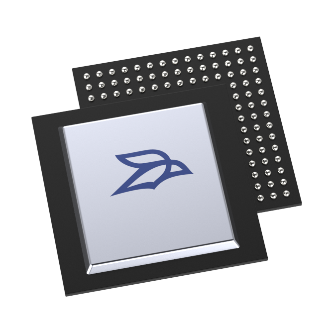
The CDRF9002 is packaged in a 12 mm × 12 mm, 196-ball chip scale package ball grid array (CSP_BGA).
CDRF9002 operates over extended industrial temperature range -40°C~+85°C.
CDRF9002 is compatible with and can replace Analog Devices, Inc.'s (ADI) ADRV9002BBCZ.

 CDRF9002BGPrice:$0.00