
introduction
In designing IoT sensors, handheld testers, and electronic scales, we often face a complex challenge: achieving three key requirements simultaneously—battery-powered operation (low voltage, low power consumption), precise measurement performance (low temperature drift), and compact size.
As a manufacturer, we fully understand the challenges engineers face during component selection: measurement errors caused by temperature drift, battery life concerns due to high power consumption, and loss of signal dynamic range at low voltages. Drawing on experience from several mass-production projects, we'll explore how zero-drift CMOS technology can effectively address these challenges with slowly varying signals in 1.8V ultra-low voltage environments.
1. When the supply voltage drops to 1.8 V, what exactly are we afraid of?
Those familiar with portable devices know that the voltage range of lithium battery power systems typically fluctuates between 1.8 V and 5.5 V.
At such low voltages, conventional operational amplifiers easily prove inadequate:
1. The signal dynamic range is limited: the power supply provides only 1.8 V. If the operational amplifier fails to operate in rail-to-rail mode, your signal will be clipped before it can be amplified.
2. Temperature drift becomes the primary source of error: battery-powered devices are often carried on the body, exposing them to significant temperature variations. The temperature drift of conventional operational amplifiers can introduce errors ranging from several tens of millivolts across the entire temperature range, which is critical for precision measurements.
3. Power consumption is the ultimate drain on battery life: every microampere (μA) of static current shortens its lifespan.
Thus, low power consumption, zero drift, and rail-to-rail operation have become the essential trio that ensures successful system selection.
II. Practical Analysis: How is a robust domestic operational amplifier manufactured?
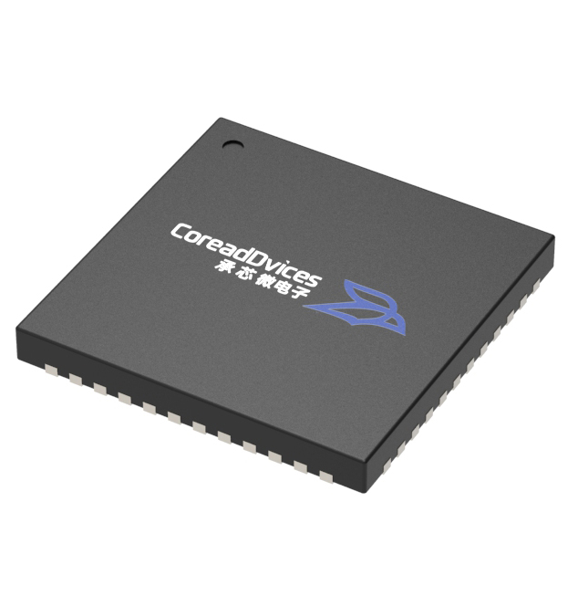
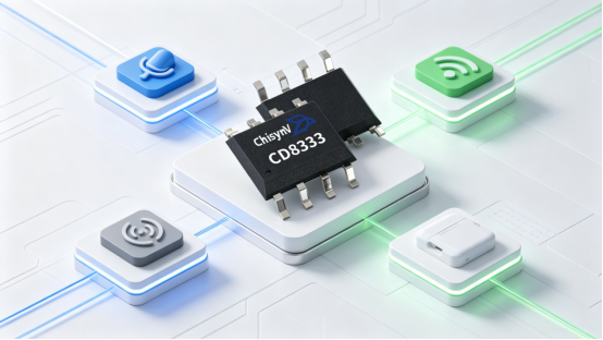
To address these challenges, the ChisynV CD8333—a single-channel zero-drift CMOS operational amplifier—has been engineered with a robust underlying architecture.
1. Power Consumption and Performance: The typical static current of a single channel is only 25 μA, falling within the standard low-power range and maximizing battery life. Utilizing chopper stabilization technology, the maximum input offset voltage at 25°C is 30 μV, with a typical zero drift of 0.05 μV/°C; signal offset remains minimal across the entire temperature range, fully meeting precision measurement requirements. Additionally, the input bias current is merely 20 pA, and its high input impedance characteristic makes it suitable for high-impedance sensors such as photoelectric and piezoelectric types.
2. Signal transmission capability: Supports rail-to-rail input/output, maximizing signal dynamic range under 1.8V low-voltage power conditions; featuring a gain-bandwidth product of 350 kHz and a voltage swing rate of 0.2 V/μs, ideal for processing mid-to-low frequency signals and compatible with slowly varying signals such as temperature, pressure, and weight measurements. The chip incorporates an integrated RF anti-electromagnetic interference filter, ensuring stable performance in complex industrial electromagnetic environments.
3. Working Environment and Limit Parameters: Standard operating temperature range-40°C to +125°C, covering conditions for both civilian and general industrial applications; maximum supply voltage of 7.5 V; ESD protection rating of 6 kV for human models, meeting the electrostatic protection requirements for conventional mass-produced products.
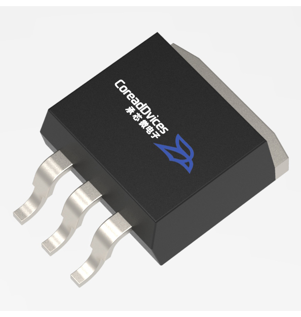
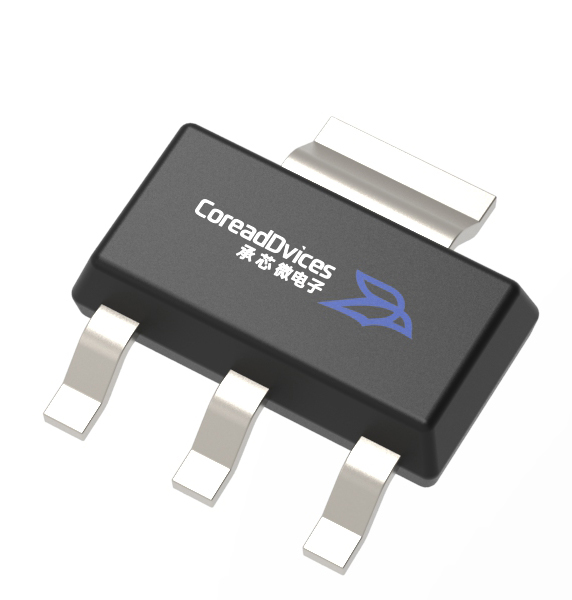
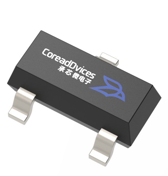
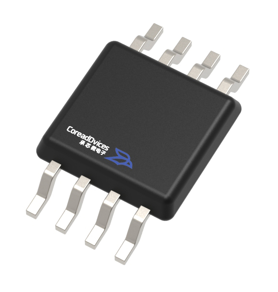
III. Packaging Selection: How to choose for different PCB applications?
This model offers three types of surface-mount packaging options, covering everything from micro-wearable devices to general-purpose industrial circuit boards, providing exceptional flexibility for mass-production designs.
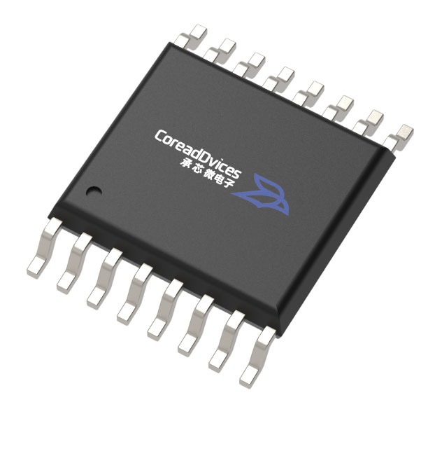
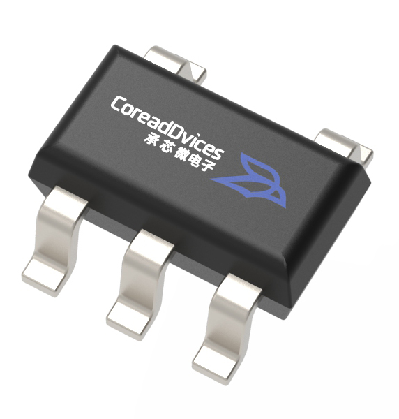
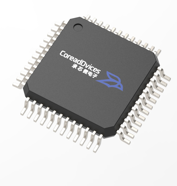
1. The SC70-5/SOT23-5 packages feature ultra-compact designs, primarily used in space-constrained applications such as fitness bands, mini thermometers, and micro-sensors, and currently rank as the two most widely shipped packaging types.
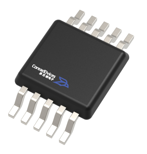
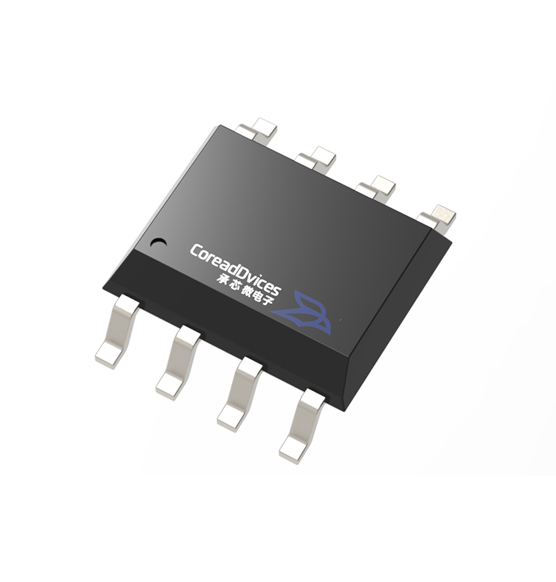
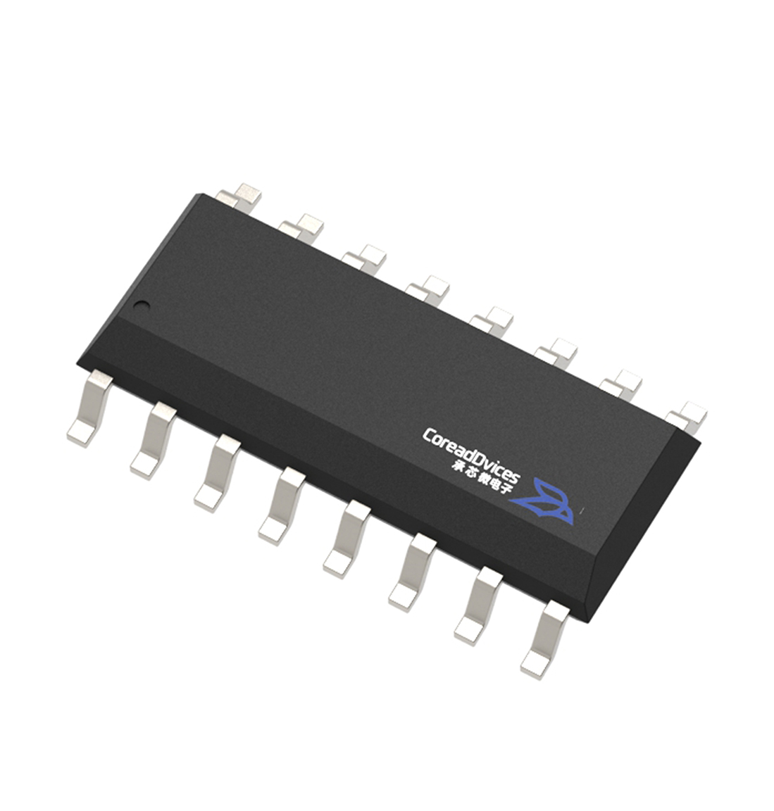
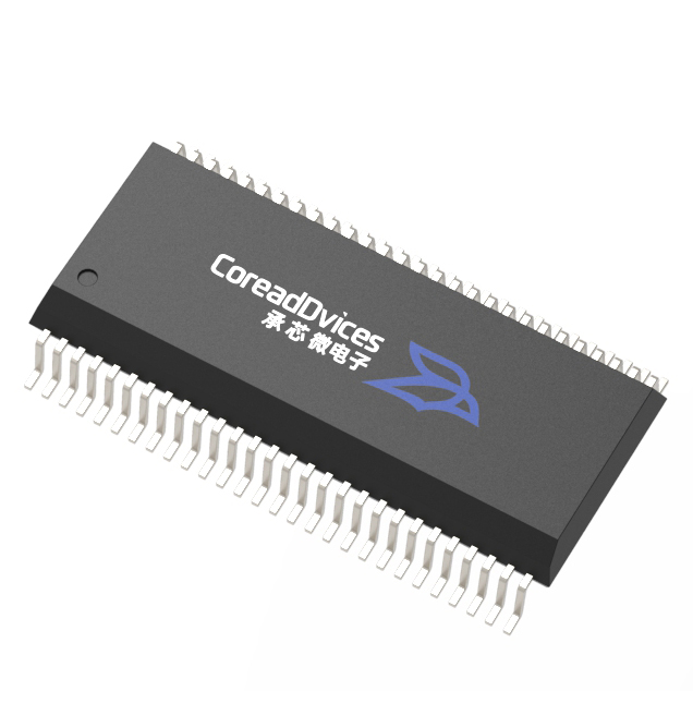
2. SOP-8: A universal standard package featuring easy soldering and debugging, ideal for conventional industrial PCBs and R&D prototypes – offering the highest versatility.
All three packaging types are standard surface-mount components, perfectly compatible with SMT automated production lines. They come in a wide range of tape winding specifications, catering to both small-batch R&D and large-scale mass production needs.
III. Hardware Design Pitfall Avoidance Guide
Based on our project debugging experience, we recommend that engineers focus on the following two design details:
1. Power bypass design: When using a single power supply, the VDD pin must be paired with a 0.1 μF ceramic bypass capacitor; in dual-power scenarios, both VDD and VSS pins should be connected to ground via bypass capacitors to ensure power stability.
2. Capacitive load handling: The CD8333 is not optimized for high-capacity loads, and directly driving capacitive loads may easily cause circuit oscillation. Two common engineering solutions are employed: first, connecting an isolation resistor in series at the output to isolate capacitive loads; second, appropriately increasing noise gain while reducing the feedback loop bandwidth.
3. Classic Application Circuits: This model enables the construction of three fundamental circuits—differential amplifiers, active low-pass filters, and instrumentation amplifiers. It is widely used for signal filtering, converting differential signals to single-ended signals, and acquiring high-impedance signals. The official manual provides complete circuit formulas for direct design implementation.
IV. Suitable Scenarios
preferred selection scenario
1. Battery-powered portable devices: handheld testers, home thermometers, electronic scales;
2. Small and medium-sized industrial sensors: analog sensor modules for temperature, pressure, and weighing applications;
3. Standard IoT wireless sensor node: a field sensing device featuring low power consumption, wide operating temperature range, and strong interference resistance.
sum up
The CD8333 is a single-channel zero-drift operational amplifier designed for precision measurement applications requiring low voltage, low power consumption, and medium-to-low frequency operation. It features a wide input voltage range of 1.8 V to 5.5 V, an ultra-low static current of 25 μA, minimal temperature drift and offset voltage, along with excellent operating performance across temperatures from-40°C to +125°C, making it ideal for battery-powered portable devices and conventional industrial sensors.
If the project requires multi-channel signal acquisition, it can be upgraded to the dual-channel CD8336 or quad-channel CD8339 within the same series, with the overall hardware design logic remaining unchanged.