
One of the most challenging requirements in signal conditioning applications is often not about achieving the highest bandwidth or maximum drive capability, but rather about meeting multiple competing demands: the weak sensor signal must not be overwhelmed by the amplifier's own offset voltage; the true output from high-impedance sensors must not be affected by additional offsets introduced by the input bias current; the battery-powered system must also ensure sufficiently low operational amplifier power consumption; and the system must operate reliably and stably throughout the entire operating range of the lithium-ion battery—from full charge to low-voltage conditions.
Traditional precision bipolar operational amplifiers often find themselves caught in a trade-off between static current and offset: reducing the offset voltage increases the static current; however, if power efficiency is a priority, the offset cannot be adequately suppressed. For designs involving high-gain, long-cycle mass production applications—such as sensor interfaces, temperature measurement systems, or electronic weighing instruments—this trade-off often has a more significant impact on actual implementation than the nominal specifications might suggest.
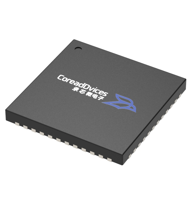
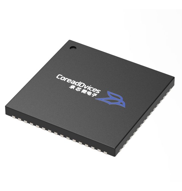
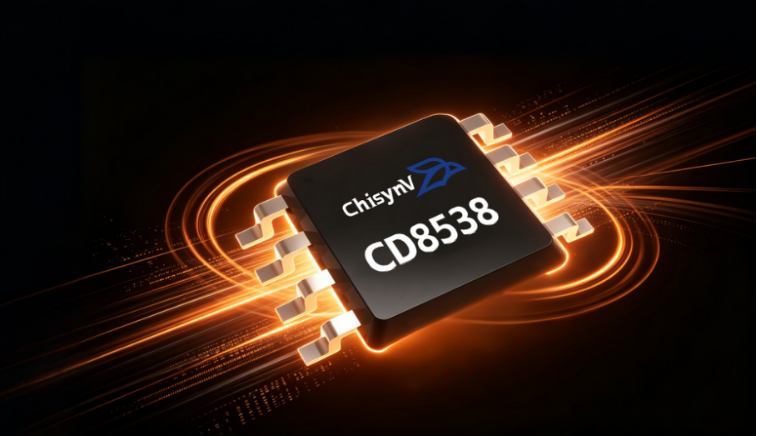
The CD8538 is a domestically produced single-channel precision operational amplifier featuring Auto-Zero (Self-Stabilizing Zero) functionality. Designed to compete with the imported AD8538, it leverages an internal auto-zero architecture to achieve extremely low offset and nearly zero temperature drift, while also offering rail-to-rail input and output capabilities, low power consumption, and industrial-grade wide-temperature operating range. This device provides a highly reliable, domestic-based signal chain solution for sensor front-end applications, portable measurement instruments, and battery-powered devices.
Architecture and Core Parameters
The CD8538 is fabricated using CMOS process technology and is designed as a general-purpose precision low-power operational amplifier. The device supports both single-power-supply operation (2.7 V to 5.5 V) and dual-power-supply operation (±1.35 V to ±2.5 V); its input common-mode range spans from 0 V to V+ (rail-to-rail input), while the output approaches the power supply rail under light-load conditions (near-rail output) and still provides a dynamic range close to the full power supply swing even when operating under low-voltage power supply conditions. The entire product family operates within a temperature range of −40°C to +125°C, qualifying it as an industrial-grade device.
Key Performance Indicators:
|
Parameter Term |
representative value |
remarks |
|
Input offset voltage Vos |
1 μV (Maximum: 5 μV) |
Automatic Zeroing Core Metric |
|
Temperature drift |
0.03 μV/℃ (Maximum: 0.05 μV/℃) |
Wide-temperature stability: -40°C to +125°C |
|
0.0110 Hz low-frequency noise |
1.3μVp p |
Ultra-low frequency noise – ideal for DC or slowly varying signals |
|
Gain–Bandwidth Product (GBW) |
1.6MHz |
Medium bandwidth – balancing accuracy and response speed |
|
Slope Rate (SR) |
0.7V/μs |
Large-signal rapid establishment |
|
CMRR / PSRR |
Up to 130 dB |
Excellent common-mode and power supply disturbance suppression capability |
|
Single-channel static current |
360 μA (Maximum: 520 μA) |
Low-power design |
|
Power Supply Coverage |
2.7 V–5.5 V (single power supply); ±1.35 V–±2.5 V (dual power supply) |
Compatible with 3.3V/5V systems and lithium-ion battery power supply |
|
working temperature |
-40℃~+125℃ |
Industrial-grade temperature rating |
|
overload recovery time |
2μs |
Upon reaching input saturation, the system quickly returns to normal operation. |
|
input bias current |
50pA |
CMOS high input impedance |
The device features stable unit gain without the need for an external phase compensation capacitor, simplifying the peripheral circuit design. Under a low-voltage supply condition of 2.7 V, its core performance remains stable, making it suitable for lithium-ion battery-powered systems.
Key engineering highlights
1. The microvolt-level off-cathode low-temperature drift serves as the baseline for the DC link.
The typical offset voltage is only 1 μV (maximum 5 μV); the typical temperature drift is 0.03 μV/°C. Over the temperature range of –40°C to +125°C (a total span of 165°C), the additional offset induced by temperature drift amounts to approximately 5 μV; when superimposed on the initial offset, the overall offset remains within the microvolt range – a critical characteristic for DC-gain-intensive links, such as those used in electronic weighing instruments or high-precision temperature measurement systems.
2. CMOS high input impedance – compatible with high-impedance sensors
With an input bias current of 50 pA, this design is suitable for signal sources with high source impedance—such as thermocouples, photodiodes, and high-impedance bridge sensors—by keeping the offset error induced by the bias current across the sensor's internal resistance at an extremely low level, thereby protecting the weak original signal from being overwhelmed by circuit noise.
3、Low power consumption and wide operating voltage range – ideal for direct battery-powered applications.
Lower operating voltage limit of 2.7 V – compatible with products powered by single-cell lithium-ion batteries or button batteries; typical single-channel static current of 360 μA – balancing accuracy and power consumption. The rail-to-rail output closely approximates the power supply voltage under light-load conditions, maximizing the ADC sampling input dynamic range and preventing small-signal clipping distortion.
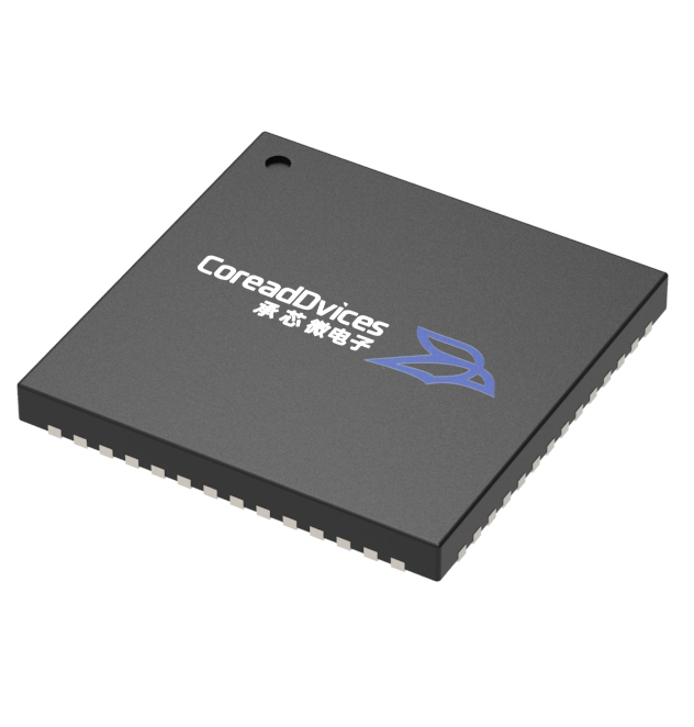
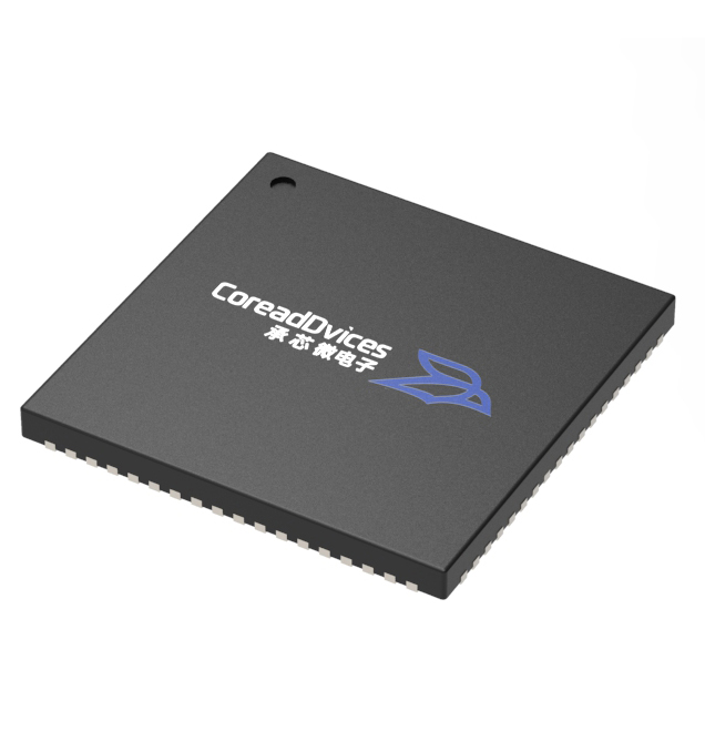
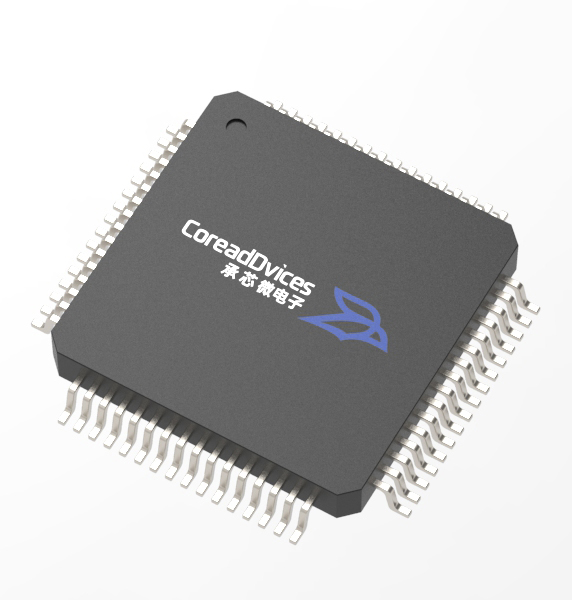
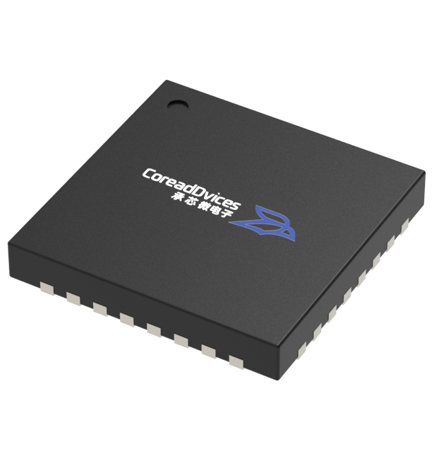
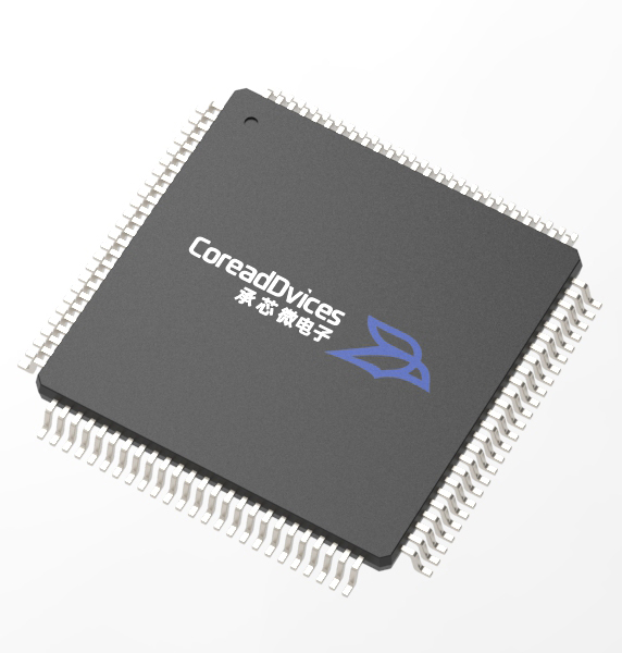
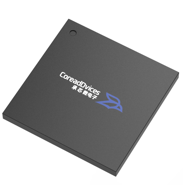
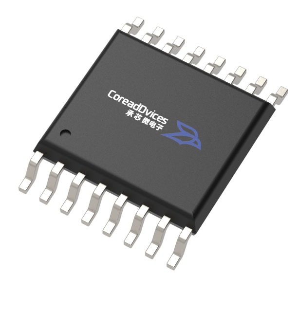
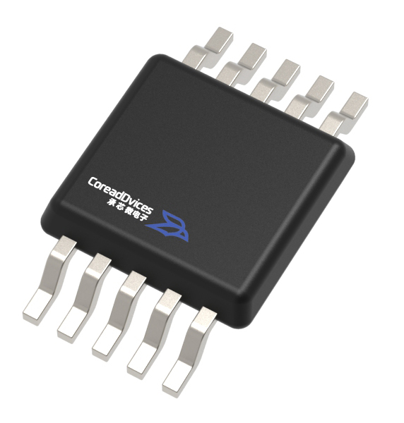
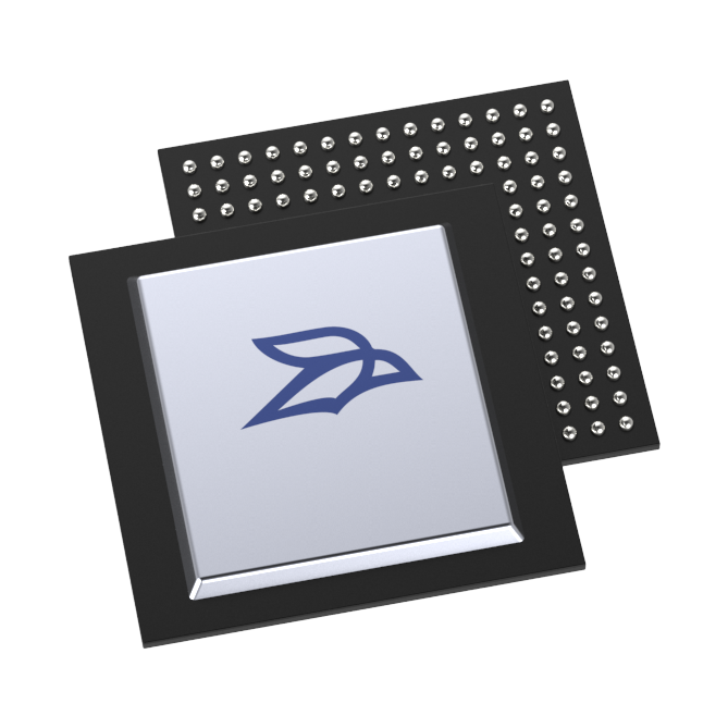
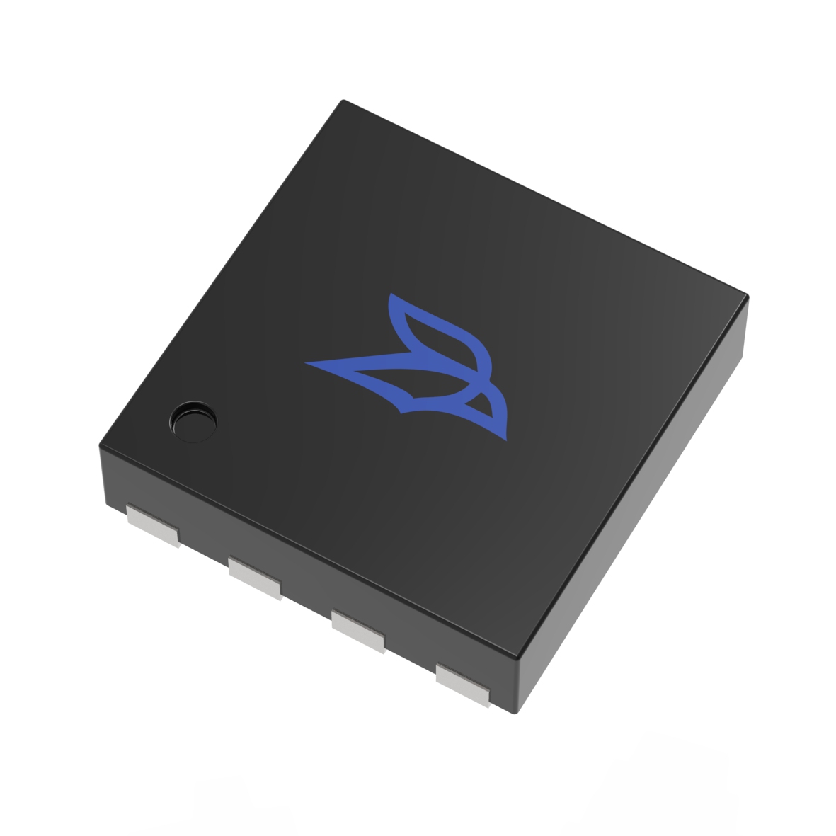
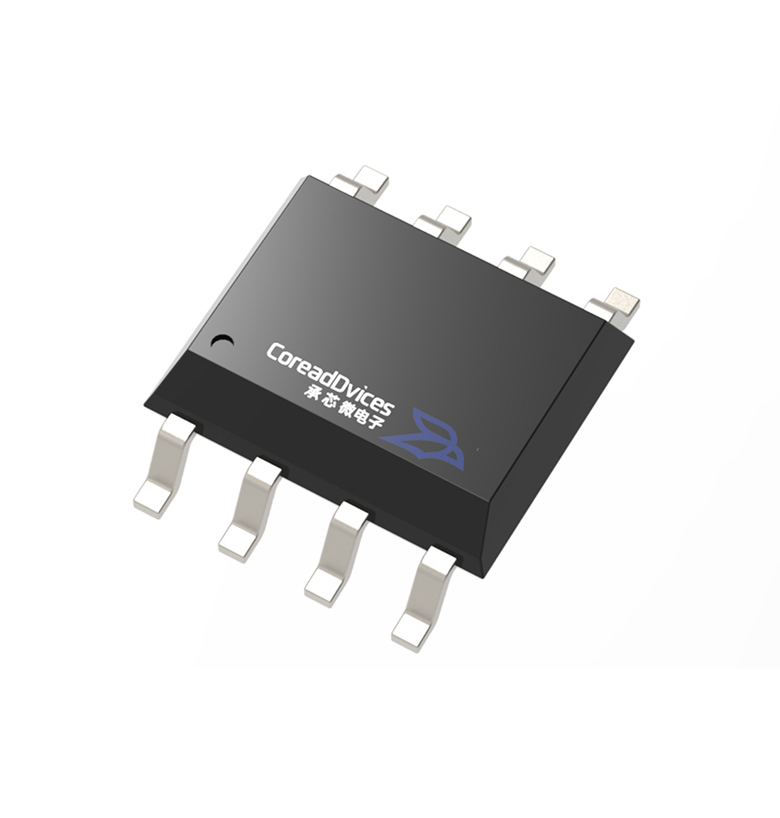
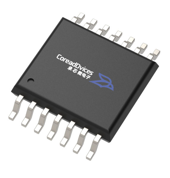
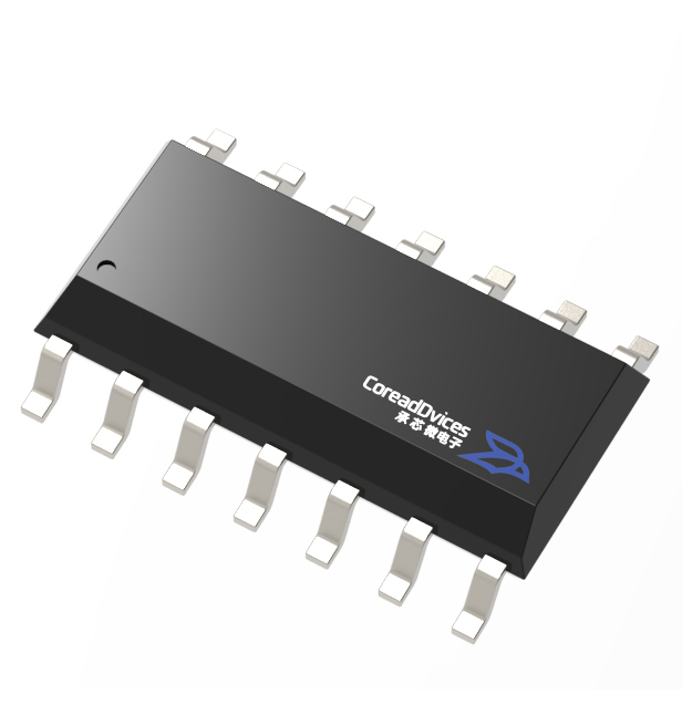
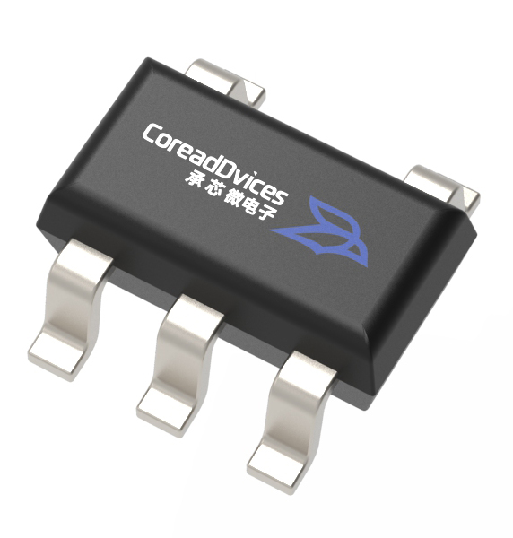
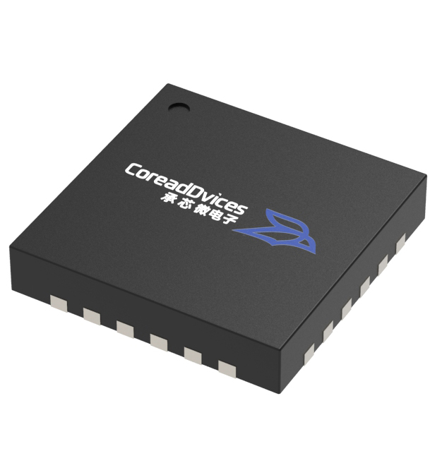
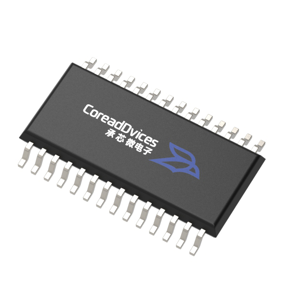
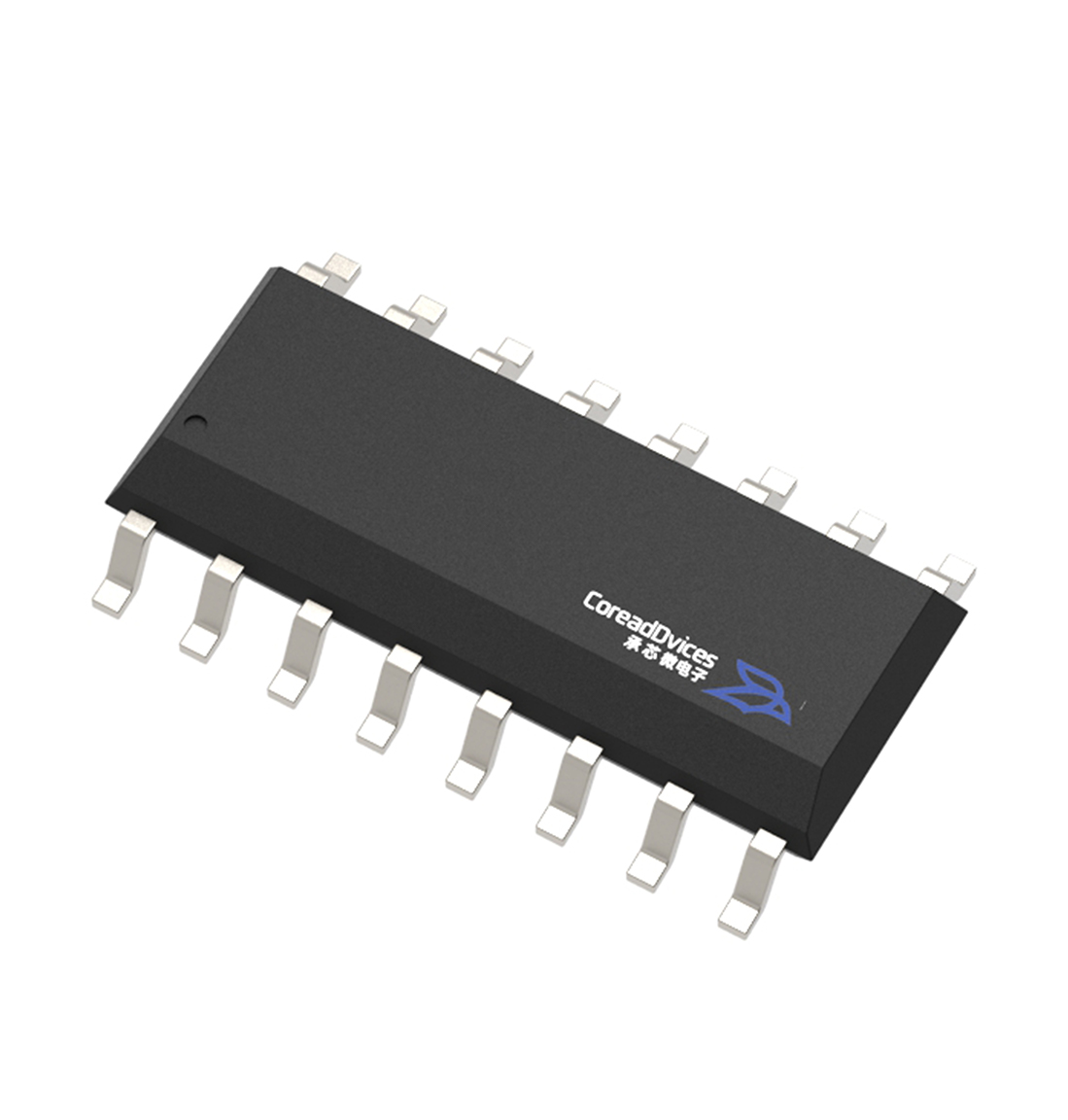
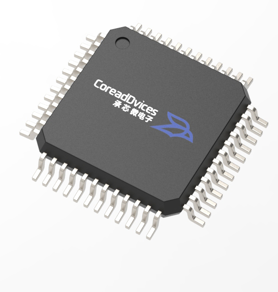
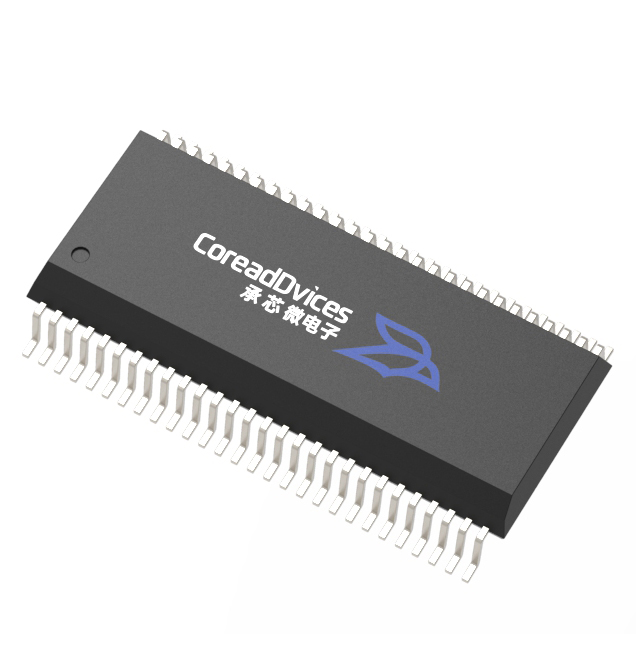
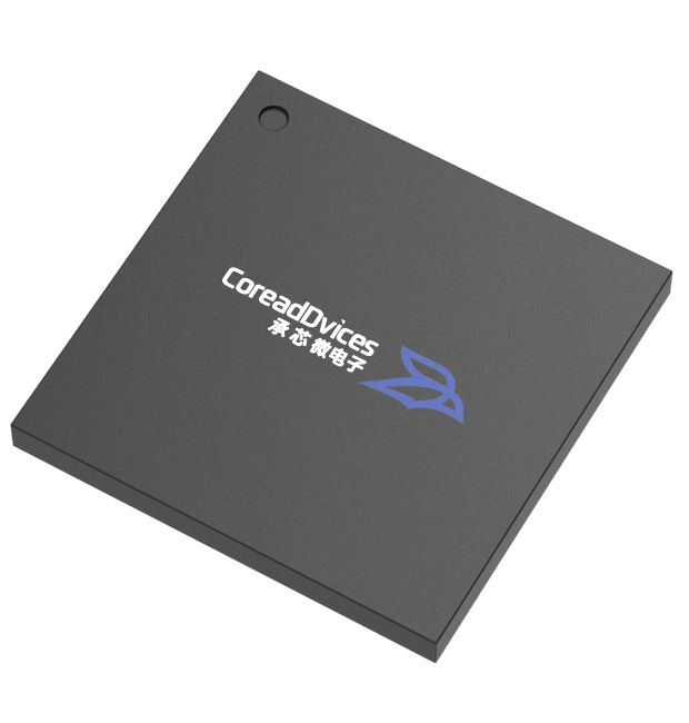
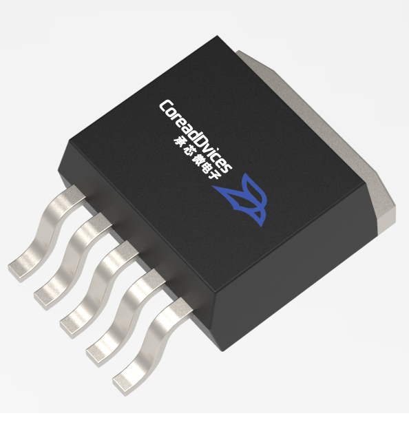
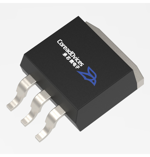
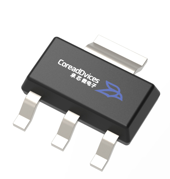
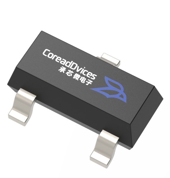
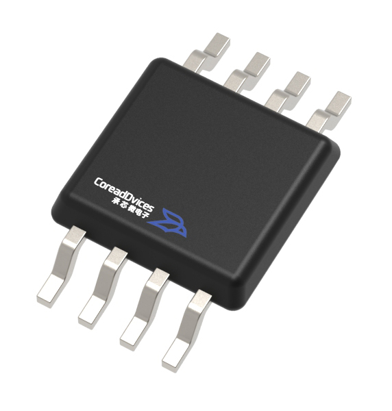
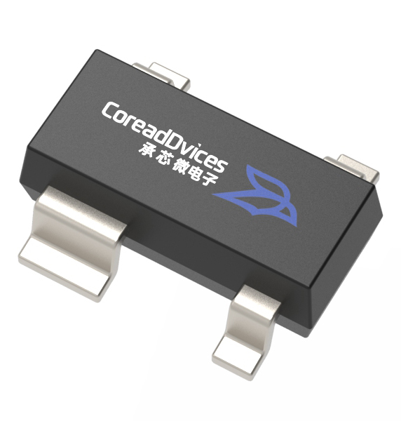
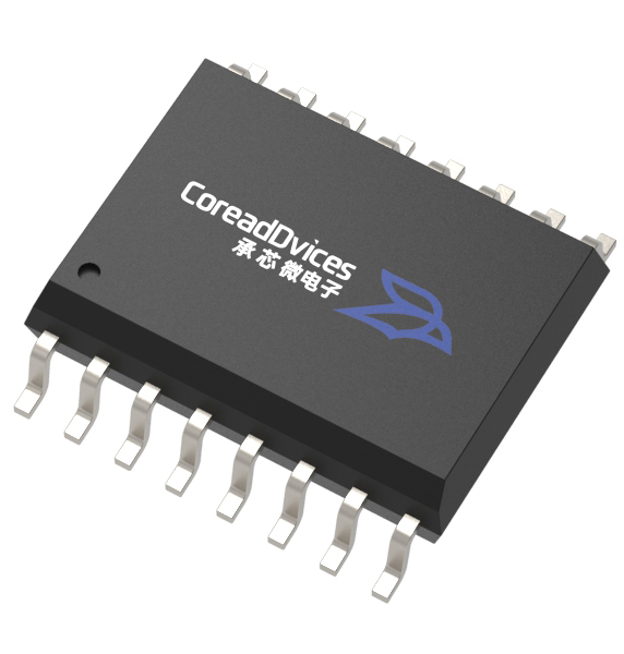
4.多样化 packaging options to meet a wide range of hardware design requirements.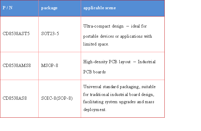
Typical implementation scenarios
CD8538 is designed for DC and low-frequency weak signal conditioning, suitable for the following equipment:
✅ Sensor signal front-end: pressure sensors, strain gauge weighing bridge circuits, thermocouple stacks, RTD/thermocouple signal amplification
✅ High-precision temperature measurement module; industrial and portable measuring instruments
✅ Portable medical testing devices, handheld data recorders
✅ Active filter, reference voltage buffer circuit
✅ Power supply sampling & inverter signal conditioning circuit
Common circuit topologies: differential amplifier, in-phase/反相 amplifier, instrumentation amplifier pre-stage, single-power-supply active low-pass filter.
Board-Level Design Key Points
The ultimate accuracy of an automatic zeroing precision operational amplifier depends heavily on its PCB implementation and the chip's superior specifications; these capabilities can only be fully realized with proper circuit layout.
1. Power supply decoupling: Place a 0.1 μF decoupling capacitor near each power supply pin to reduce power supply noise interference.
2. Suppression of PCB thermoelectric potential (Seebeck effect): Keep input signal traces as short as possible; implement symmetrical, equal-length routing for the input differential paths; where necessary, incorporate a Guard Ring layout; avoid direct exposure of input nodes to airflow to prevent additional errors introduced by local temperature variations. Contact interfaces between dissimilar metals can induce an additional drift of more than 0.1 μV/°C, which can nullify the chip's inherent low-temperature drift advantage.
3. Input overvoltage protection: When the input signal exceeds the power supply rail by more than 0.5 V, external current limiting is required to ensure that the input current is ≤ 10 mA.
4. Load stability: For larger capacitive loads, it is recommended to include a series isolation resistor in the output circuit.
5. Product Description: This chip is designed for DC low-frequency precision measurement with a bandwidth of 1.6 MHz; it is not suitable for high-frequency AC signal processing.
The boundary that requires an objective understanding
The CD8538 is designed for precision DC and low-frequency signal conditioning, rather than high-speed amplification. With a gain-bandwidth product of 1.6 MHz, it is suitable for DC to several tens of kHz signals; for applications above the audio range that require ultra-fast settling times, a higher-bandwidth op-amp should be selected. This device features an automatic zeroing architecture; however, a small amount of clock-related stray noise may be present due to the internal chopping circuit – this can be mitigated by applying RC filtering during the backend ADC sampling phase. The noise level between 0.01–10 Hz is 1.3 μVp–p, which meets the requirements of the vast majority of precision measurement applications; for applications demanding extremely low noise levels, the component selection should be re-evaluated. Even when the chip drift is extremely low, it is still recommended to maintain a small calibration margin in the overall system to compensate for errors arising from PCB thermoelectric effects or the sensor itself.
Model Selection Summary
If you are involved in sensor signal conditioning, industrial instrumentation, or portable measurement devices and are facing significant zero drift or high temperature drift errors while seeking to reduce the need for external calibration circuits, the CD8538 is an excellent, cost-effective domestic precision operational amplifier option.