
In modern electronic systems such as industrial automation, the Internet of Things (IoT), and smart medical devices, the demand for processing precise analog signals has become increasingly urgent. As core components of these systems, signal amplifiers must ensure high precision while maintaining low power consumption and excellent environmental adaptability. However, many existing operational amplifiers on the market often struggle to achieve this balance. Some products have high power consumption that fails to meet the requirements of battery-powered systems; others experience performance degradation in environments with significant temperature fluctuations; while traditional single-channel designs occupy excessive PCB space, increasing system complexity and costs.
The CD8339 from ChisynV is a four-channel, low-power, zero-drift CMOS operational amplifier. By leveraging chopper stabilization technology and optimized parameter design, it achieves a perfect balance of high precision, low power consumption, and high integration, providing reliable underlying support for high-impedance and low-offset applications.
Core parameters implemented
In terms of power supply and power consumption, the CD8339 supports single-supply operation from 1.8V to 5.5V, with an absolute maximum supply voltage of 7.5V. It features overvoltage fault tolerance, enabling direct compatibility with mainstream power solutions like lithium batteries and low-voltage linear power supplies without requiring traditional dual-supply configurations. This significantly simplifies low-voltage system power circuit design, reduces the number of power management components, and effectively lowers BOM costs. Each amplifier has a typical static current of only 25μA, with a total four-channel current of merely 100μA—dramatically lower than conventional operational amplifiers of equivalent performance. This design significantly extends battery-powered devices' operational lifespan, reduces reliance on external power for field operations, and enhances overall equipment efficiency.
The precision advantage stands as a core competitive edge of the CD8339. Powered by chopper-stabilized technology, this product achieves an input offset voltage of up to 10μV (25℃) and zero drift of 0.05μV/℃ (typical value). Within the industrial-grade temperature range of-40℃ to +125℃, the precision drift remains negligible, effectively preventing temperature-induced measurement errors, reducing equipment calibration frequency, and lowering operational costs. Additionally, its 20pA typical input bias current and 10pA typical input offset current ensure signal integrity in high-impedance sensors without attenuation, maintaining signal fidelity without additional buffering circuits and enhancing system measurement resolution. The 110dB Common Mode Rejection Ratio (CMRR) and 115dB Power Supply Rejection Ratio (PSRR) effectively suppress power noise and environmental common-mode interference, guaranteeing pure output signals without requiring extra multi-stage filter designs.
The CD8339 delivers a 350kHz gain bandwidth product (GBP) of +100 at 25°C, enabling full coverage of slow-changing sensor signals in the mid-low frequency range through closed-loop gain conversion. This design achieves optimal balance between performance and cost while effectively suppressing high-frequency noise. Its rail-to-rail output ensures near-power-supply voltage output under 5V operation with minimal voltage swing across loads, maximizing dynamic range in low-voltage systems. The ADC driver eliminates the need for additional conditioning circuits, streamlining the "op-amp + ADC" signal chain. To address common capacitive load oscillation issues, the manual provides two engineering solutions: a series isolation resistor and noise gain enhancement, accommodating capacitive loads without extra buffers to improve system stability.
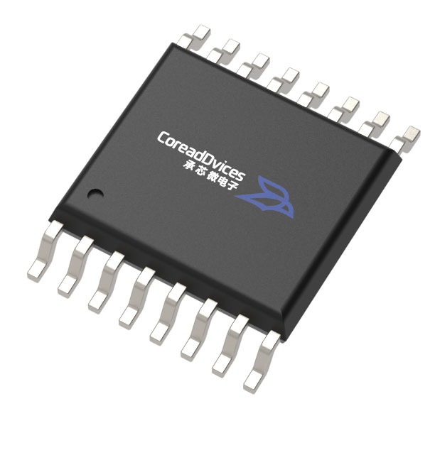
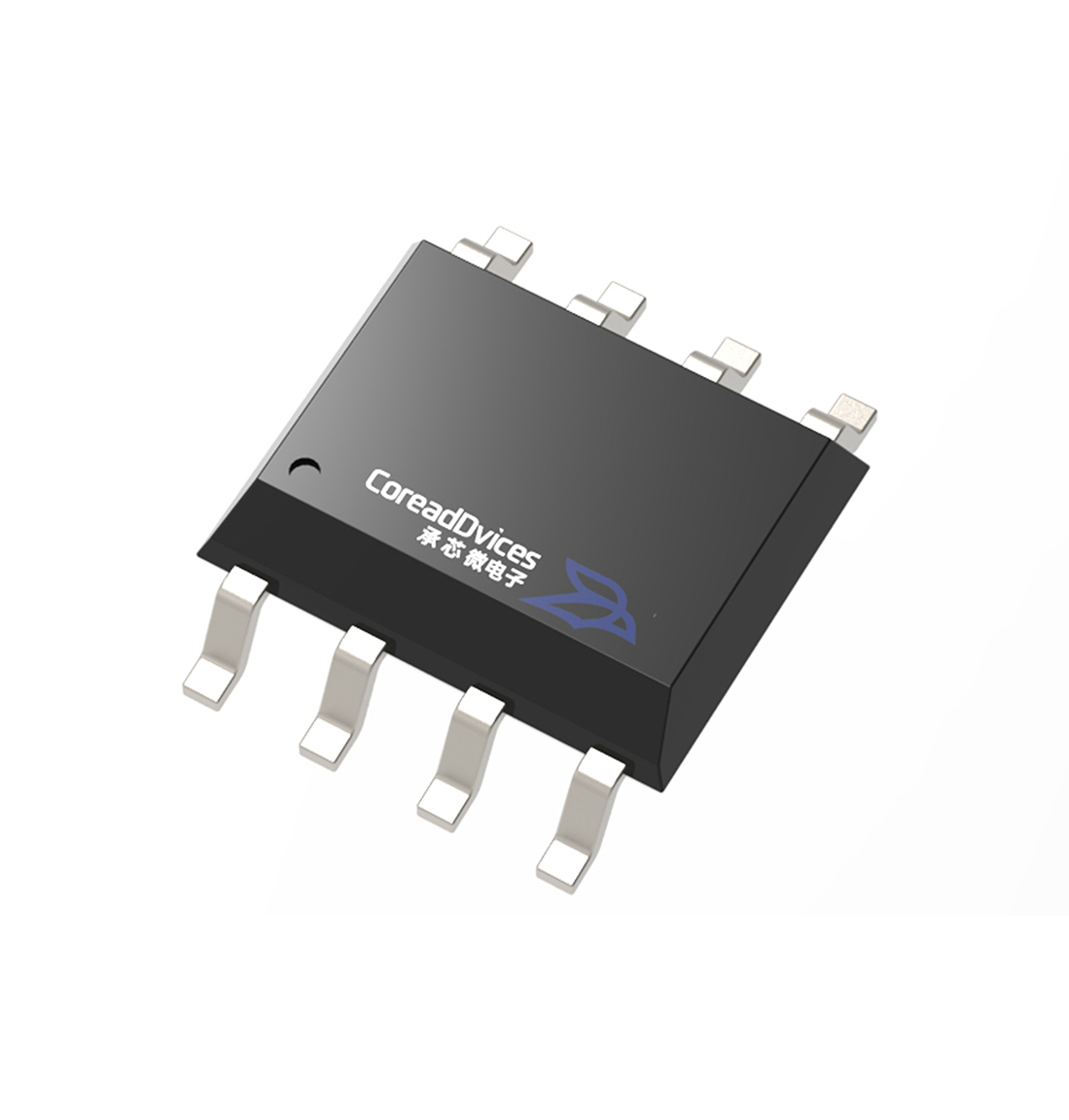
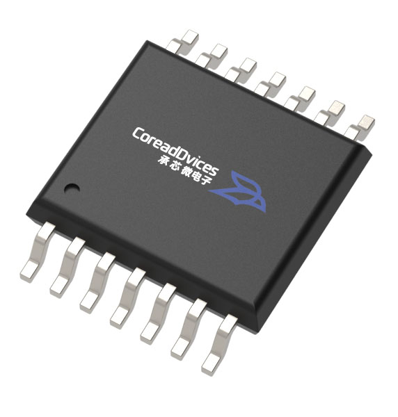
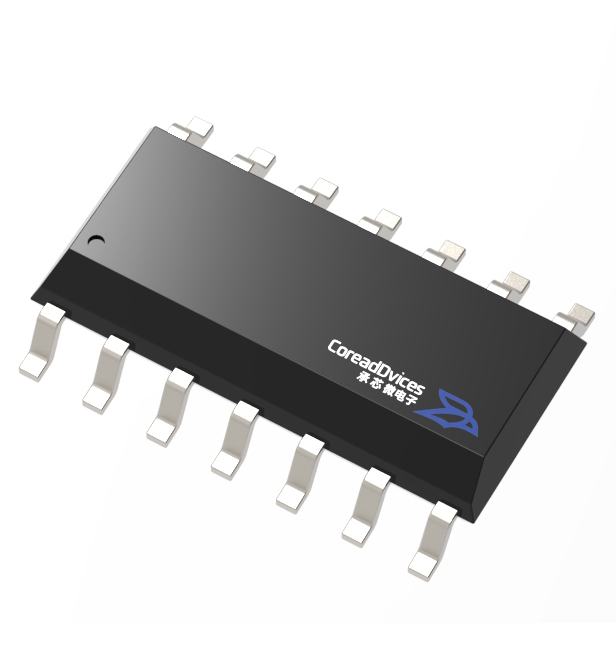
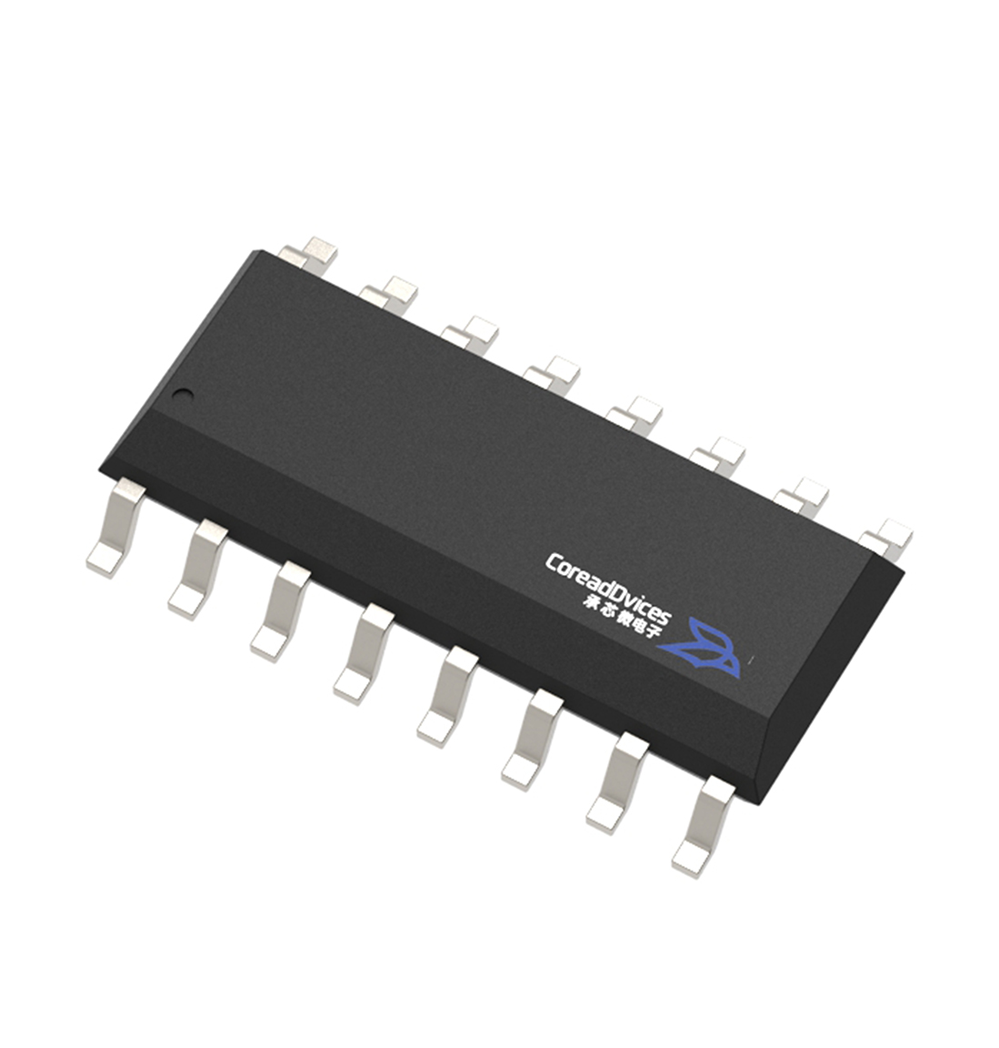
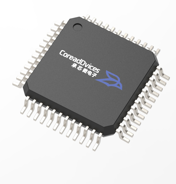
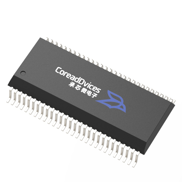
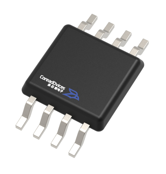
The anti-interference and packaging design significantly expand the product's application scope. The CD8339 features an integrated RF EMI filter that effectively suppresses external radio frequency interference, eliminating the need for additional EMI filtering components. This simplifies circuit design while saving PCB space. Available in two packaging options—SOIC-14 (SOP-14) and TSSOP-14—both meet mass production requirements for storage and soldering. The product offers 6kV human model ESD protection and 400V machine model ESD protection, with a maximum node temperature of 160°C, storage temperature range of-55°C to +150°C, and soldering temperature (within 10 seconds) up to 260°C, ensuring reliable performance in harsh environments and mass production processes.
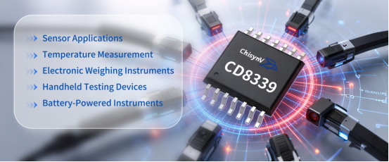
Typical application
Industrial sensor signal conditioning: featuring low offset voltage, stable performance across wide temperature ranges, and high anti-interference capability, it meets the signal amplification requirements of various industrial sensors while ensuring signal fidelity and measurement accuracy.
Electronic weighing instruments: The four-channel integration reduces component count, with high common-mode rejection ratio (CMR) to mitigate environmental interference and ensure weighing linearity.
The handheld testing device features low-power consumption to extend lithium battery life, a compact design for lightweight operation, and built-in EMI filters to ensure stable test data.