
I. Industry Background and Product Positioning
In analog front-end designs such as precision sensing signal conditioning, low-voltage battery-powered systems, and industrial multi-channel acquisition, DC accuracy, power consumption control, dynamic range, and temperature-wide performance consistency have become critical selection criteria. In practical engineering applications, traditional operational amplifiers often suffer from issues including significant offset voltage and temperature drift, the need for additional calibration for weak signal amplification, insufficient output swing under low-voltage single-power-supply conditions, and challenges in achieving unified parameter specifications across multi-channel architectures—all of which directly increase system design complexity and risks to mass production consistency.
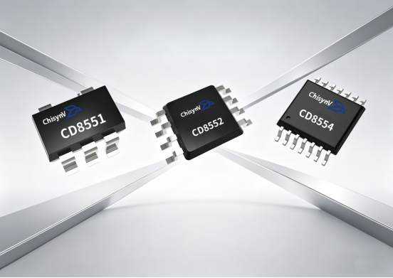
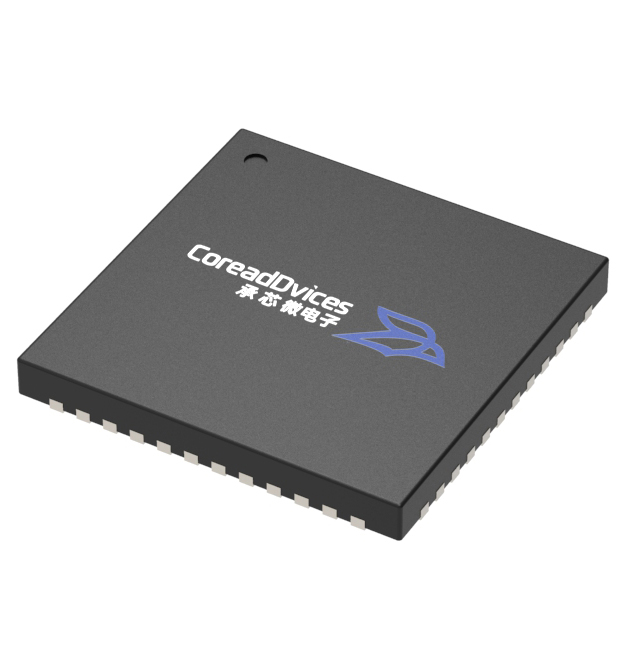
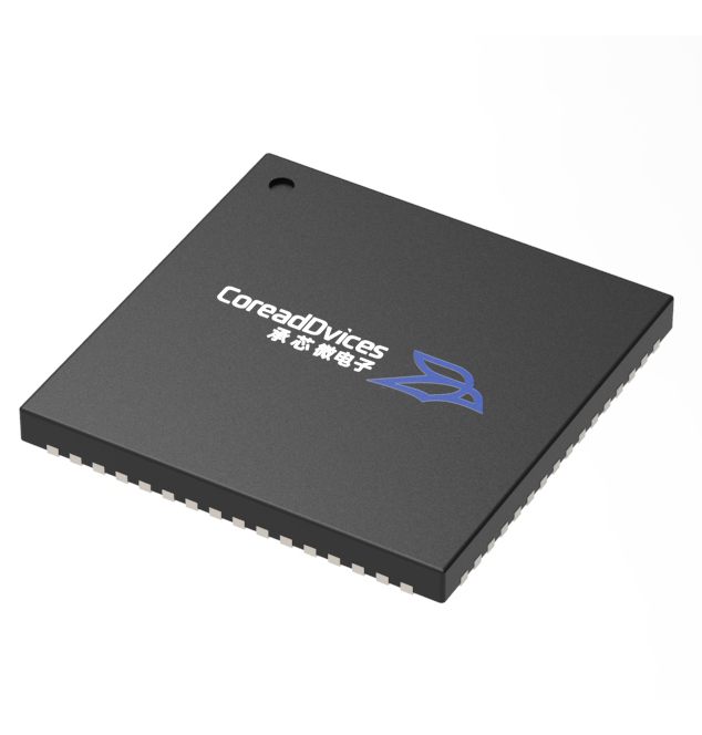
The ChisynV Microelectronics CD8551/CD8552/CD8554 series are zero-drift CMOS operational amplifiers with single-, dual-, or four-channel configurations, fabricated using a chopper-stabilized process. Designed as industrial-grade, high-precision, low-power, rail-to-rail universal precision op-amps, they deliver standardized performance parameters to meet diverse precision signal processing requirements, providing engineers with a one-stop solution for component selection.

II. Core Features
The CD855X series employs chopper stabilization technology, delivering industry-leading DC accuracy and anti-interference performance. At 25°C, the typical input offset voltage is 1 μV; across the full temperature range of-40°C to +125°C, the typical input offset voltage drift is 0.005 μV/°C, enabling near-zero drift signal amplification throughout the temperature spectrum. Both the common-mode rejection ratio and power supply voltage rejection ratio reach 130 dB, while the typical gain for high signal voltages is 135 dB, effectively suppressing common-mode interference and power supply fluctuations to ensure high-fidelity acquisition of microvolt-level weak signals and maintaining excellent differential linearity when driving ADCs. Additionally, the product features low input bias current and noise characteristics: a typical input bias current of 50 pA at 25°C, voltage noise of 0.75 μVp-p across 0.01 Hz to 10 Hz, and voltage noise density of 35 nV/√Hz at 1 kHz, making it suitable for high-impedance inputs and low-frequency precision measurement applications.
The product supports single-power-supply operation at 2.7V–5.5V and is compatible with dual-power-supply configurations ranging from ±1.35V to ±2.75V. With a typical single-channel static current of 640μA, it achieves optimal balance between low-voltage operation and low power consumption. The series features comprehensive rail-to-rail input/output performance, extending the input common-mode voltage range to VSS–0.1V–VDD+0.1V while delivering near-rail output swing. It maintains excellent output swing capability under both 100kΩ high-resistance and 10kΩ medium-resistance loads, maximizing the dynamic range of low-voltage systems. This design meets full-range signal processing requirements without requiring a dual-power architecture, significantly simplifying hardware power supply design.
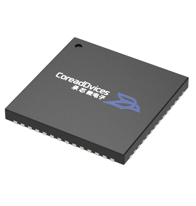
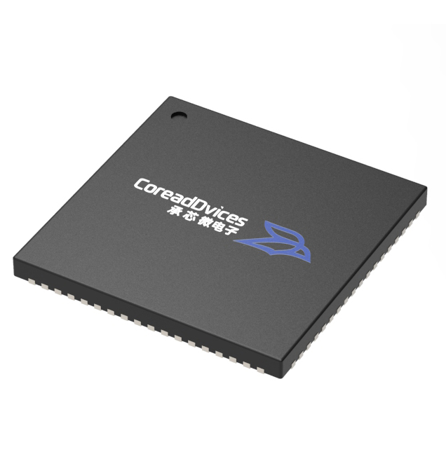
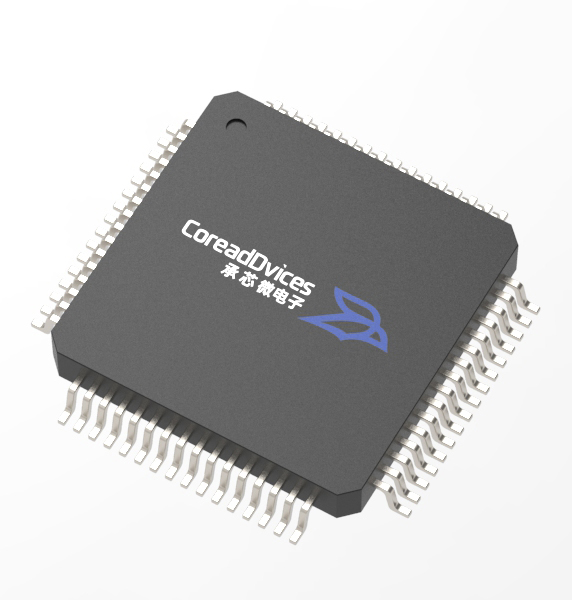
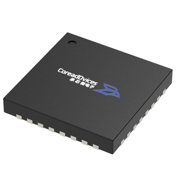
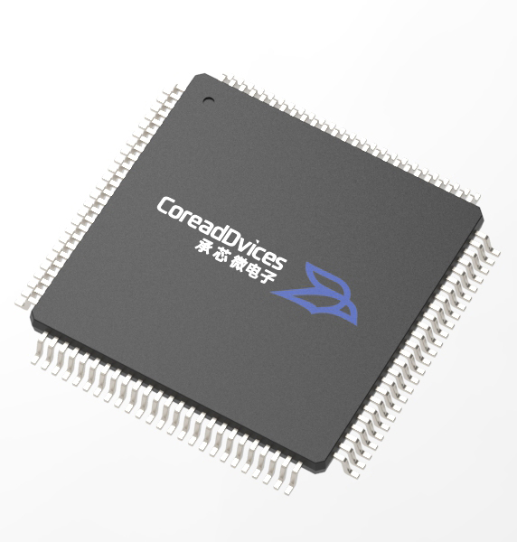
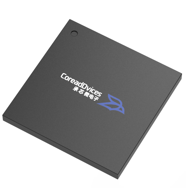
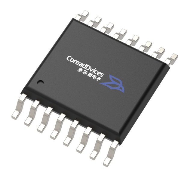
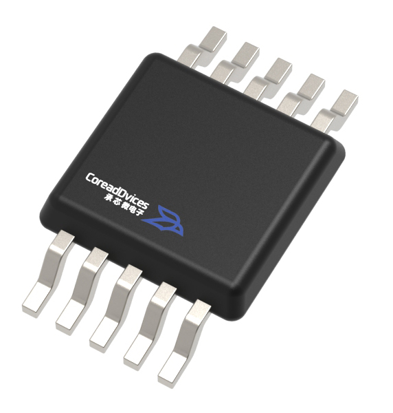
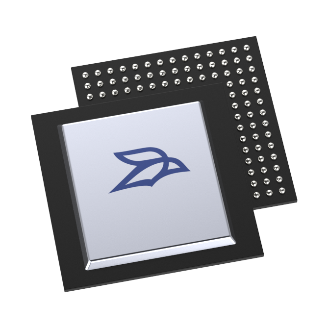
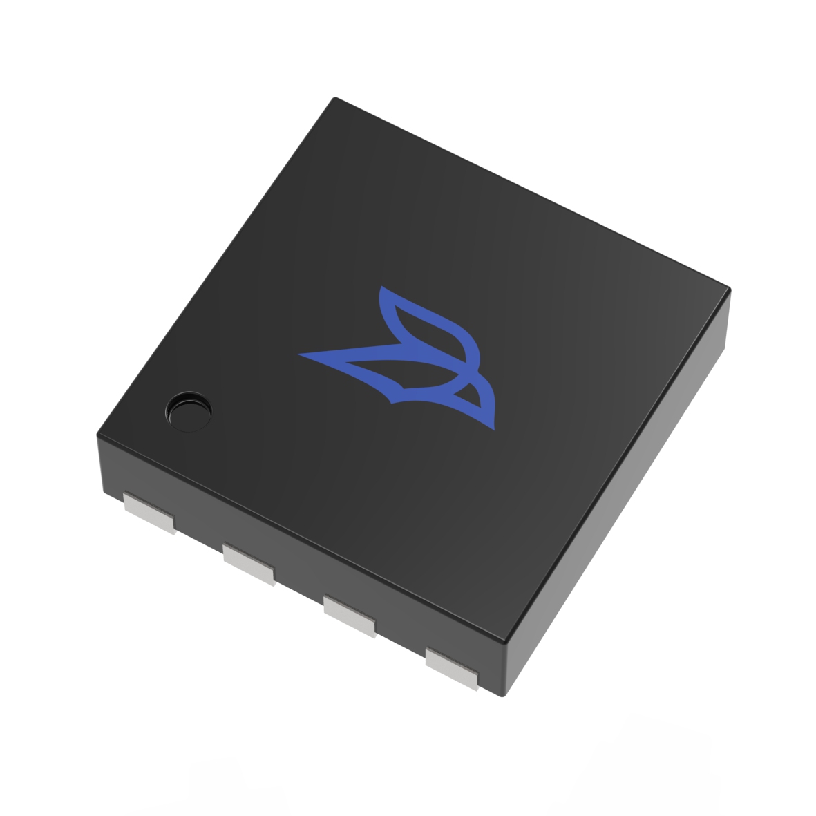
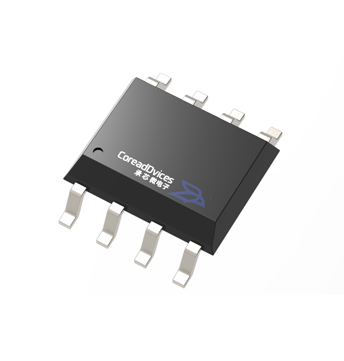
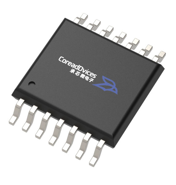
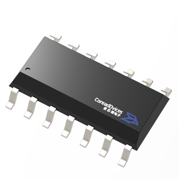
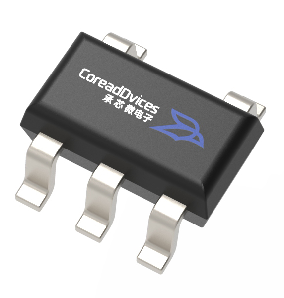
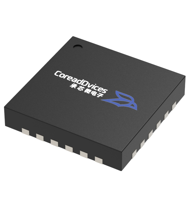
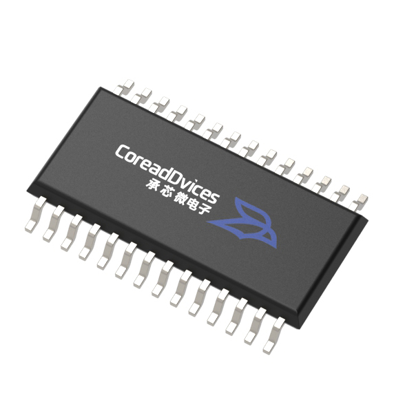
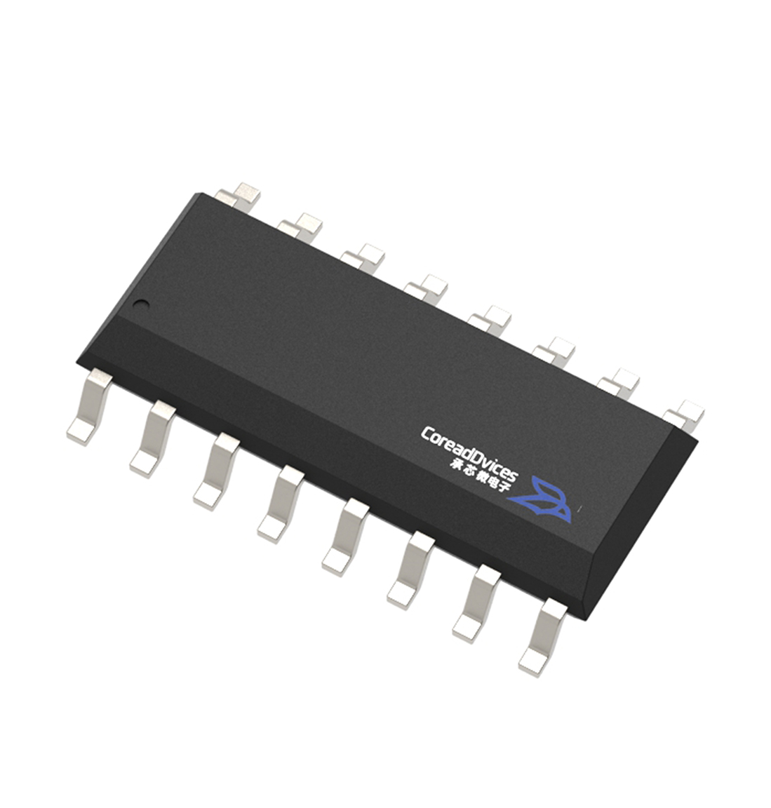
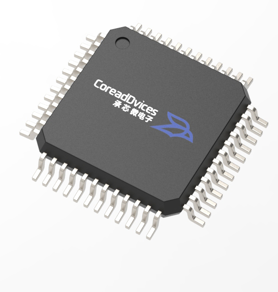
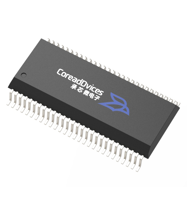
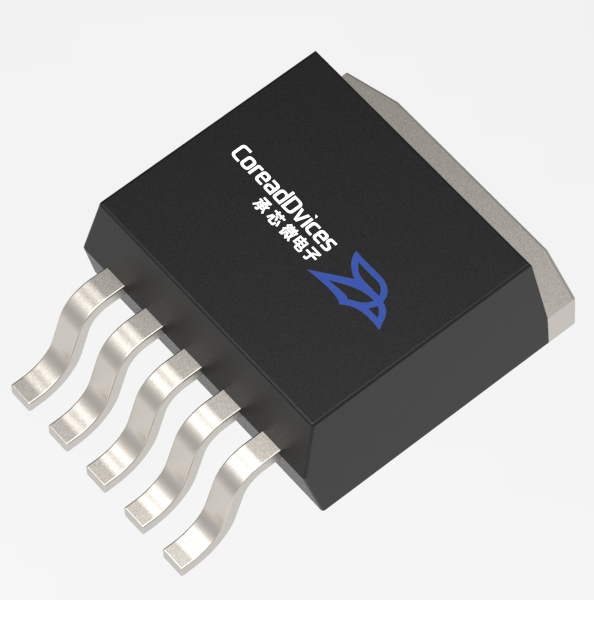
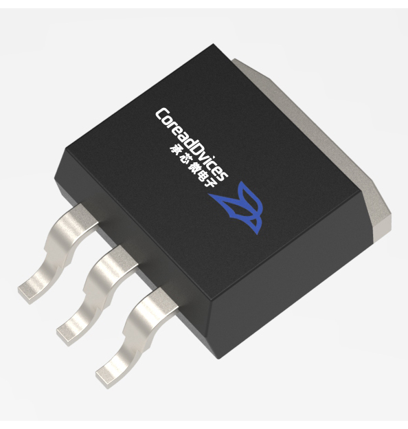
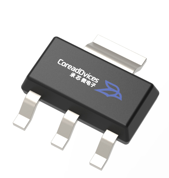
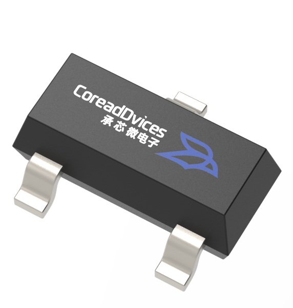
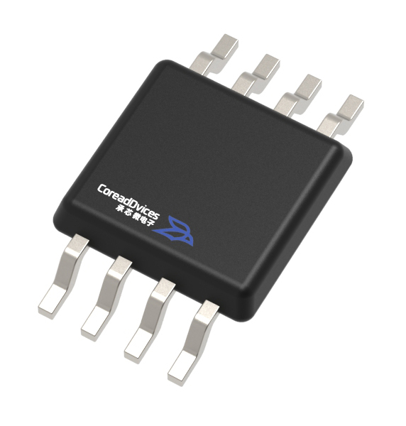
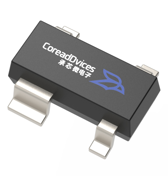
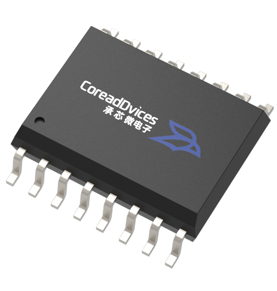
The series features dynamic performance equilibrium with typical gain-bandwidth product values of 5 MHz, voltage conversion rates of 1.9 V/μs, and overload recovery times of 0.05 ms, meeting response speed requirements for applications such as active filtering and dynamic signal acquisition. The product delivers industrial-grade reliability, operating within a temperature range of-40°C to +125°C, with ESD human model withstand capability of 5 kV and maximum power supply voltage tolerance of 7 V, enabling adaptation to harsh industrial environments. It offers flexible single-, dual-, or four-channel configurations and is available in various package types—including SOT23-5, SOP-8, MSOP-8, TSSOP-8/14, and SOP-14—which balance compact PCB layout with multi-channel signal processing requirements, making it ideal for high-density integration and multi-link acquisition system designs.
III. Typical Application Scenarios
l Battery-powered portable instrument: Leveraging its wide-voltage and low-power consumption characteristics, it is designed for handheld detection and portable measurement devices, extending battery life and simplifying power supply design.
l Precision sensor signal amplification: Compatible with weighing, temperature, pressure, and strain gauge sensors, ensuring zero drift and low offset for accurate signal amplification and enhanced measurement precision.
l Medical/Industrial Precision Instruments: Featuring high immunity to interference, low noise, and stable performance across wide temperature ranges, these instruments meet the precision and reliability requirements for medical testing and industrial online monitoring.
l Signal conditioning circuit: Compatible with source filtering, differential amplification, and instrumentation amplification circuits, with bandwidth and noise characteristics tailored to meet signal conditioning requirements.
l ADC Drive and Power Conversion: A high-linearity ADC driver that preserves differential linearity, compatible with the signal conditioning stages of power converters and inverters.