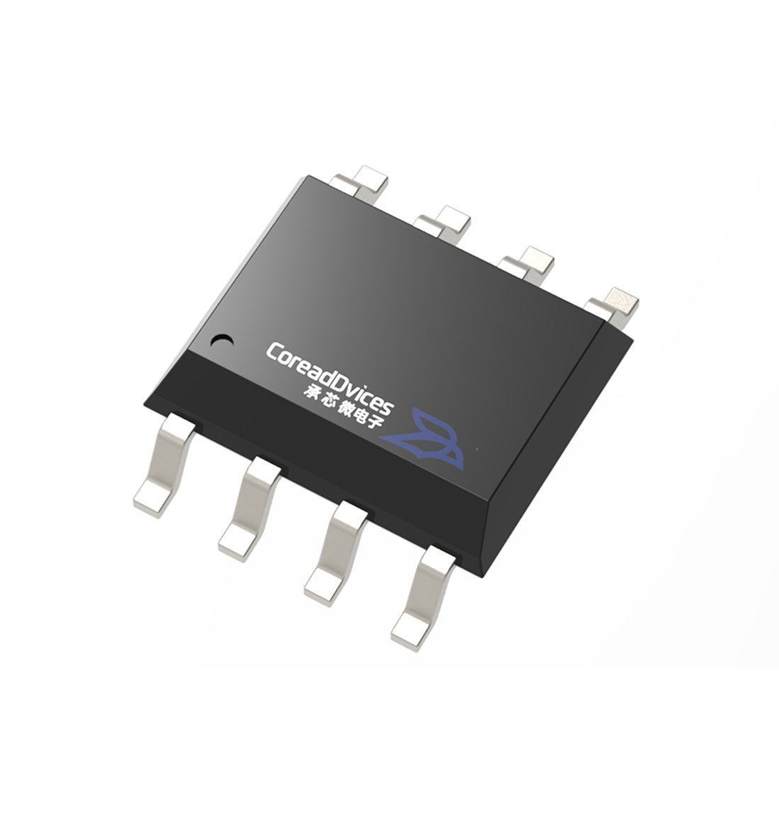
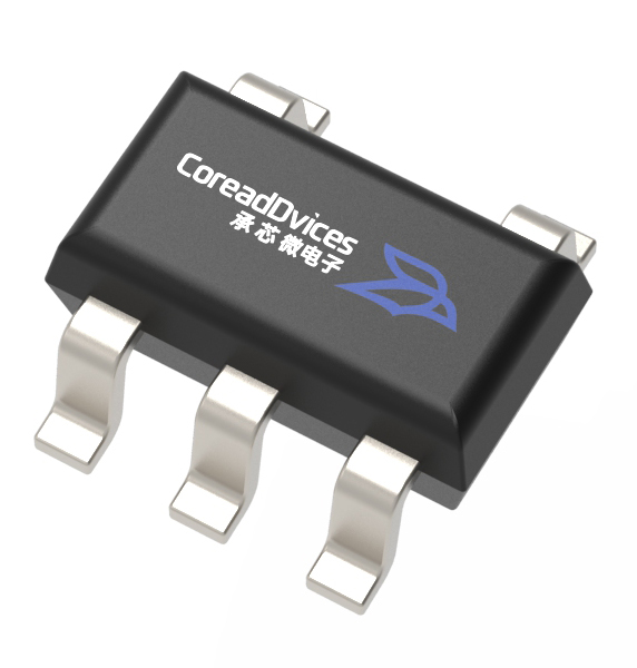
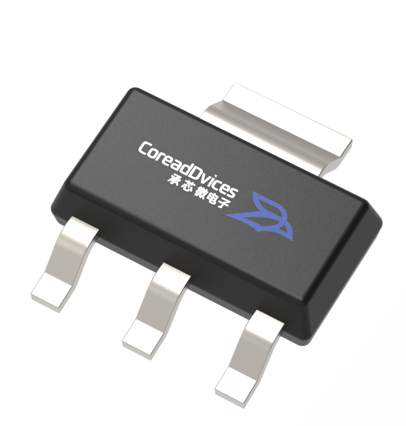
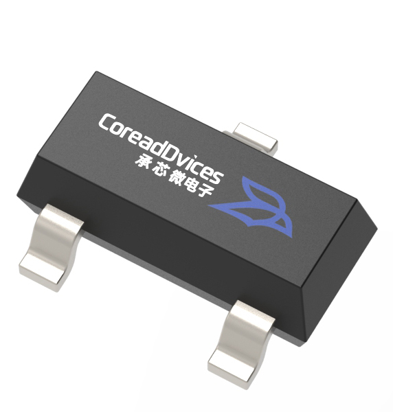
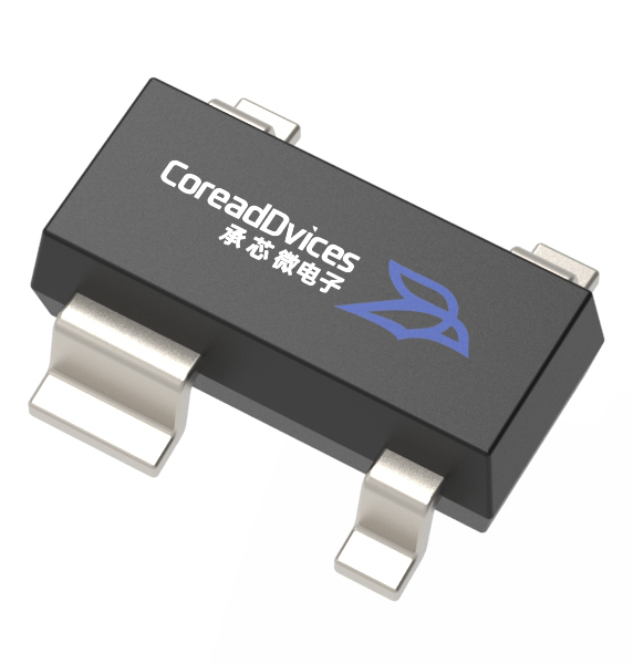

ChisynV Micro's solution to this type of requirement is the CD812—a high-level-active microprocessor monitoring circuit. It integrates precision threshold comparison, power-on reset delay, and anti-bounce manual reset into a single four-pin small package, providing six reset threshold levels (L/M/T/S/R/Z) specifically designed for nominal power supplies of 5 V, 3.3 V, 3.0 V, and 2.5 V. It is intended for embedded designs requiring reliable reset, such as MCU systems, smart instruments, and portable measurement devices.
Device Architecture and Key Parameters
The CD812 internally consists of a threshold comparator, a reset timer, a debouncing circuit, and an output stage. The comparator continuously monitors VCC; when VCC falls below the threshold of the selected mode, it drives the RESET line high within approximately 40 µs. Once VCC crosses the threshold, the internal timer allows the reset output to remain active for a specified period before it is released; this constitutes the power-on reset delay. RESET is active on high level and is connected to pin 2; the manual reset (MR) pin is located on pin 3, is internally pulled-up, and can be triggered by pulling an external button pin low; internal debouncing ignores narrow glitches.
The following are the key electrical characteristics at 25 °C (the full temperature range is listed separately in the threshold table):
|
parameter |
condition |
representative value |
Range / Maximum Value |
unit |
|
Monitor power supply voltage |
— |
— |
1.0 ~ 5.5 |
V |
|
source current |
— |
5 |
15 (maximum) |
µA |
|
Reset threshold L |
25℃ |
4.63 |
4.54~4.72 |
V |
|
Reset threshold M |
25℃ |
4.38 |
4.30~4.46 |
V |
|
Reset threshold T |
25℃ |
3.08 |
3.03~3.14 |
V |
|
Reset threshold S |
25℃ |
2.93 |
2.88~2.98 |
V |
|
Reset threshold R |
25℃ |
2.63 |
2.58~2.68 |
V |
|
Reset threshold Z |
25℃ |
2.32 |
2.28~2.35 |
V |
|
Reset threshold temperature coefficient |
— |
30 |
— |
ppm/℃ |
|
MR minimum pulse width |
— |
10 |
— |
µs |
|
MR Edge Suppression |
— |
100 |
— |
ns |
|
MR to reduction transmission delay |
— |
0.5 |
— |
µs |
|
Power supply voltage to reset delay |
— |
40 |
— |
µs |
|
Reset timeout |
— |
240 |
140~560 |
ms |
|
The reduction remains effective until |
VCC drop (explicitly guaranteed for the CD811) |
— |
1.0 |
V |
|
RESET outputs a low level |
ISINK=1.2mA(R/S/T/Z) |
— |
0.3 (maximum) |
V |
|
RESET outputs a low level |
ISINK=3.2mA(L/M) |
— |
0.4 (maximum) |
V |
|
RESET outputs a high level |
ISOURCE=150µA |
0.8×VCC |
— |
V |
|
working temperature |
— |
— |
−40 ~ +85 |
℃ |
|
package |
— |
— |
SOT-143-4 |
— |
Four key aspects of the project: polarity, threshold, power consumption, and manual reset
A high-level reset output corresponds to one specific design category. The CD811 in the same series provides a low-level reset, whereas the CD812 provides a high-level reset; the primary difference between the two lies in the polarity of the reset output. For output capability at low voltage, please refer to the specific model specifications. In the CD812, a high-level RESET signal indicates that reset is active; it can be connected to a high-level active reset input. Once the voltage has recovered and the reset delay has elapsed, the output is released from reset. If the MCU's reset input is low-level active, the CD811 is a more suitable choice. These two options belong to the same class; the choice should be made based on the polarity of the downstream reset signal.
Six-stage thresholds are compatible with mainstream rated power supplies.
|
gear |
25 °C typical threshold (V) |
Full temperature range (V) |
|
L |
4.63 |
4.50~4.75 |
|
M |
4.38 |
4.25~4.50 |
|
T |
3.08 |
3.00~3.15 |
|
S |
2.93 |
2.85~3.00 |
|
R |
2.63 |
2.55~2.70 |
|
Z |
2.32 |
2.25~2.38 |
The reset threshold temperature coefficient is 30 ppm/℃; when selecting the component, the threshold range across the entire temperature range should also be verified.
Low power consumption and wide-voltage monitoring directly determine battery life. With a typical power supply current of 5 µA, the monitor covers a wide voltage range from 1.0 V to 5.5 V while consuming virtually no battery capacity; the reset output remains active during power loss (the CD811 explicitly guarantees operation down to VCC as low as 1 V; the low-voltage hold capability of the CD812 should be verified for the specific model), and it does not exhibit threshold-related jitter or false triggering upon power-up.
Manual reset is integrated onto the chip. Internally, the MR has a 10/20/30 kΩ pull-up; externally, simply pull the button directly to GND. The on-chip debouncing ignores noise spikes shorter than 100 ns; a low level that persists for more than 10 µs is considered a valid reset. No explicit guarantee is provided for signal handling within the range of 100 ns to 10 µs. This makes the device suitable for scenarios involving button bounce and line noise pickup.
Applicable Scenarios and Corresponding Model Selection
MCU System and Controller: Power-on, power-off, and undervoltage reset for the 3.3 V/5 V embedded main controller.
Smart meters and portable measurement: electricity meters and handheld instruments, featuring low power consumption and wide-temperature compatibility for field operating conditions.
Safety and in-vehicle peripherals: Assessability for related peripheral applications; automotive-grade/functional safety certification and EMI immunity requirements must be confirmed on a project-by-project basis.
Equipment requiring manual reset: MR integrates the manual restart function into a single chip, eliminating the need for a discrete reset-button circuit.
Scope and Applicable Preconditions of the CD812
The CD812 provides fixed-threshold precision monitoring; the threshold is determined by the suffix level and cannot be adjusted. If the system's nominal voltage falls outside the six available levels, the margin must be reassessed or a different level must be selected. The maximum reset timeout is 560 ms; if the system requires a longer reset hold time, a delay can be added in the firmware or an external extension circuit can be used. ESD at 3 kV represents the basic level; sensitive production lines still require standard protection. It does not provide window comparison, watchdog functionality, or adjustable delay, as these requirements are not part of its design objectives.
Key Considerations for Board-Level Design and Load Calculation
It is recommended to place a 0.1 µF ceramic decoupling capacitor near the VCC pin to reduce the risk of unintended reset caused by ripple. The MR internally integrates a pull-up resistor, so the pin can be left unconnected; if an external button is connected to GND, the trace length should be kept short, and long traces should be shielded or placed in series with a resistor to suppress noise pickup. RESET is active high; when 1.8 V <VCC <VTH(MIN) and ISOURCE = 150 µA, it outputs a high level of approximately 0.8 × VCC, allowing direct drive of a high-level-active MCU; if the downstream stage requires a low-level-active signal, an external inverter should be added. The typical reset timeout is 240 ms, with a specified range of 140–560 ms; please calculate the worst-case value based on the system boot time.
Six-stage thresholds and 5 µA micro-power consumption: Why the CD812 deserves to be included in the BOM
Based on the above analysis, the value of the CD812 lies in three key aspects: the convenience of high-level reset output for direct drive of high-effective-MCU applications; the reset determinism provided by six threshold levels combined with a temperature drift of 30 ppm/℃; and the contribution of its 5 µA micro-power consumption and reset hold during power loss to battery life and safety. For teams developing MCU systems, smart instruments, or portable measurement solutions, this four-pin monitoring circuit offers a domestically produced option with well-defined parameters and minimal peripheral requirements. When selecting the part, first confirm which threshold level the reset polarity of the subsequent stage corresponds to relative to the nominal voltage; then evaluate whether the reset timeout and temperature range meet site requirements; and finally verify packaging compatibility.